Bus Pirate 6 · Volume 8
Bus Pirate 6 Volume 8 — The Adapter Ecosystem (Probe Cable, WSON8/DIP8/SOP8, KF141, Aux, Planks)
Engineer-grade detail on the cables and adapters in the kit + the broader plank ecosystem (DDR5, SIM, PS/2, custom proto)
8.1 About this volume
This volume is engineer-grade detail on every piece of physical hardware that mates with the BP6’s probe header — the accessories in the kit, what other accessories exist, what they’re good for, what their gotchas are. Read this when you’re about to use one of the flash adapters, when you’re considering buying more adapters, or when you’re designing a custom plank.
The eight accessories cataloged in Vol 1 § 7 get one section each in §§ 2-9. The broader Where Labs ecosystem and community alternatives are in §§ 10-11.
Vol 9 walks the workflows that use these adapters end-to-end; this volume is the reference.
8.2 The Probe Cable Set (BP5-PROBE-REV2)
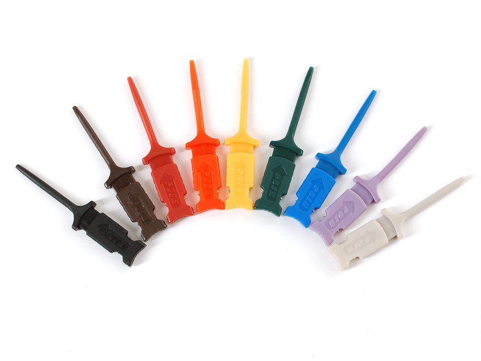
The standard cable kit — $9.95 at shop.buspirate.com. Identical SKU regardless of BP version (5, 5XL, 6); the probe-header pinout is the same across all generations.
A note on terminology: this kit is sometimes referred to in marketing copy as the “Premium Probe Cable Kit” — the “premium” descriptor refers to the silicone-jacketed 22 AWG wire (vs the cheaper PVC-jacketed kits some other vendors ship). It’s the same SKU as the standard “Probe Cable Set.”
8.2.1 TJC8A keyed locking connector — pinout
The cable terminates on the BP6 side in a TJC8A (also designated HX25418) keyed locking 10-pin connector. Pin pitch 2.54 mm. The housing has a polarized keyway so the connector physically only inserts in one orientation.
Pinout matches the BP6’s 10-pin probe header (Vol 2 § 11.1):
Table 1 — Pinout matches the BP6's 10-pin probe header ([Vol 2 § 11.1](/bus-pirate-6/vol-2/#2111-main-probe-header--tjc8a-10-pin-keyed-locking))
| Pin | Function | Cable color |
|---|---|---|
| 1 | VOUT / VREF (PSU output) | Red |
| 2 | IO0 | Orange |
| 3 | IO1 | Yellow |
| 4 | IO2 | Green |
| 5 | IO3 | Blue |
| 6 | IO4 | Purple |
| 7 | IO5 | Brown |
| 8 | IO6 | Gray |
| 9 | IO7 | White |
| 10 | GND | Black |
Important: pin-to-IO mapping is hardware-fixed, but IO-to-protocol-role mapping is mode-dependent. The color White (IO7) is MOSI in SPI mode (Vol 6 § 5.2), but it’s an arbitrary IO in I²C mode (Vol 6 § 4.2). There is no universal “brown = MOSI” or similar — the role depends on the active mode.
8.2.2 22 AWG silicone cable spec
The cable wire is 22 AWG silicone-jacketed, 60-strand tinned copper. This is significantly higher-quality wire than the typical 28 AWG PVC of cheap DuPont jumpers — it’s flexible (silicone doesn’t get stiff at low temperatures), more resistant to fatigue (60 strands vs the 8-12 of cheap wire), and lower-resistance per length.
Total cable length from connector to probe-end DuPont crimps: 270 mm.
The probe-end terminations are unhoused 2.54 mm DuPont female crimps, wrapped in heat-shrink that color-coordinates with the wire. Unhoused means you can plug directly onto a male pin without an intermediate connector — but it also means the crimps aren’t physically protected, so don’t bend them too sharply.
8.2.3 Cable colors per IO
The color map in § 2.1 is the canonical one. Don’t memorize “brown = MOSI” — memorize “brown = IO5.” When SPI is active, IO5 happens to be CS, so brown is CS. When SPI mode is reconfigured (the user changes the default pin assignment), brown follows IO5 — which might now be something else.
The same goes for every wire color. Map cable color → IO number; let the mode tell you what role that IO has.
8.2.4 Bundled starter hooks + milled breadboard pins
The Probe Cable Set ships with two bundled accessories — bundled with the cable, not separate SKUs:
- 10 starter hooks — small black IC test-hook style, designed to grab SMT IC leads or PCB component leads. Generic Shenzhen-made; serviceable for casual prodding but not high-end.
- 10 milled breadboard pins — solid square-pin headers turned from copper-nickel, milled square in the middle so they don’t roll off the bench. Each pin mates the BP DuPont female ↔ a 2.54 mm breadboard hole or 0.1″ male header.
The milled pins solve a real problem: the stranded silicone wire of the cable, when plugged directly into a breadboard, fatigues the breadboard contacts over many insertion cycles. The solid milled pins are durable and avoid that wear.
Use the starter hooks for “I want to grab onto an SMT pin briefly” cases. Use the milled pins for “I’m building a breadboarded test fixture I’ll leave in place.” Different tools for different jobs.
8.2.5 Aftermarket upgrade candidates (E-Z-Hook, Pomona)
The starter hooks are good enough for most work but wear out after a few hundred insertions. When they do:
- E-Z-Hook XKM — premium-tier IC test hook from a Long-Beach, CA manufacturer. ~$1-2 per hook. Significantly stronger spring, gold-plated contacts, smaller jaw for fine-pitch SMT.
- Pomona 3784 — another premium hook with similar specs.
- Pomona 6244 — micro-grippers (smaller jaw, better for 0.5 mm-pitch SMT than test hooks).
Where Labs doesn’t sell these — third-party purchase from DigiKey, Mouser, or direct from the manufacturer. The transition is gradual: keep the starter hooks for casual use, buy 3-4 premium hooks for the work where a slipped probe is expensive.
8.3 WSON8 SPI flash adapter ($15.95)
For desoldered WSON-8 packaged SPI flash chips. WSON (Wettable-flank Small Outline No-lead) is the modern, smaller, lead-less successor to SOP-8 — common on BIOS/UEFI flash in modern motherboards, IoT routers, embedded cameras.
8.3.1 The clamshell socket — 5×6 mm and 6×8 mm WSON-8
The adapter has a spring-loaded clamshell retainer with a lift-and-lock clip. It accepts both common WSON-8 footprints:
- 5×6 mm WSON-8 — smaller footprint, 0.5 mm pitch under-bottom pads. Common on smaller flash capacities (1-8 Mbit).
- 6×8 mm WSON-8 — larger footprint, same pad architecture. Common on larger capacities (16-64 Mbit) and on parts that need better thermal dissipation.
Chip orientation: pin 1 indicator is silkscreened on the adapter PCB. Match the chip’s pin 1 (corner dot or notch) to the indicator. Wrong orientation will short-circuit the chip if power is applied.
8.3.2 Target chip families (BIOS / UEFI / router flash)
The adapter is designed for standard 25-series SPI NOR flash in WSON-8. Confirmed compatible families:
- Winbond W25Q series (W25Q16/32/64/128/256) — most modern PC BIOSes
- Macronix MX25 series
- Cypress (Infineon) S25
- Adesto / Dialog AT25
- Microchip SST25 / SST26
- ISSI IS25LP
The adapter ships with a W25Q80DVZPIG sample chip (an 8 Mbit Winbond) so you have a known-working part to verify the socket works.
Use cases:
- BIOS / UEFI flash on x86 motherboards — modern boards mostly use WSON-8 for the SPI flash that holds the firmware. Dump → patch → re-flash workflow.
- IoT router / camera firmware — many ESP-class consumer devices have WSON-8 main flash.
- Custom embedded designs — any board you’re developing that uses WSON-8 flash benefits from out-of-circuit programming on this adapter.
8.3.3 The PCM12 voltage-routing switches
The adapter has small DIP switches that route the chip’s WP (Write Protect) and HOLD pins differently per chip family. Some chips use these as protection inputs that need to be tied high for normal operation; others use them as Quad-SPI data lines for chips supporting QSPI mode.
The default switch position works for most 25-series flash. If a particular chip family expects different routing — typically documented in the chip’s datasheet — flip the relevant switches.
The PCM12 switches don’t matter for stock SPI flash dump workflows. They matter when:
- The chip uses Quad-SPI (4-bit data) instead of single SPI
- The chip has hardware write-protect that needs to be defeated
- The chip uses non-standard pinout
For 99% of dump/verify/write tasks, accept defaults.
8.3.4 Out-of-circuit only — why you can’t clip a WSON
WSON packages are lead-less — the contacts are flat pads on the underside of the chip. There’s nothing for a clip to grab onto.
Consequence: to read a WSON-8 flash chip, you must desolder it from the target board. Hot-air rework station, board temperature ~250°C, lift the chip, place in this adapter, dump.
For in-circuit reading of WSON parts, you’d need:
- A test point for each SPI signal exposed elsewhere on the target board (rare), or
- A micro-grabber clip on each WSON pad (mechanically extremely fiddly; cheap WSON probes exist but are unreliable), or
- A dedicated WSON-8 in-circuit programmer (some exist; expensive).
The standard answer is “desolder it” — uncomfortable but reliable. Practice on junk PCBs before doing it on a board you care about.
8.4 DIP8 SPI flash adapter ($5.95)
For through-hole DIP-8 packaged SPI flash. DIP-8 is a 2010-era and earlier package; new chip families don’t ship in DIP-8 anymore, but dev boards, vintage computers, and many maker projects still socket DIP-8 flash chips.
8.4.1 The 16-pin aquamarine ZIF socket
The adapter is built around a 16-pin DIP-16 ZIF (Zero Insertion Force) socket with a lever. The DIP-8 chip socketed into one half of the 16-pin opening — pins 1-4 in one row, pins 5-8 in the corresponding socket pins.
ZIF means: lift the lever, drop the chip in (zero force), close the lever, chip is held firmly. No insertion wear, no pin damage from misalignment.
The DIP-8 sits in the “upper” 8 pins of the socket (silkscreen-labeled), leaving the lower 8 pins unused. Pin 1 corner is silkscreened — match the chip’s pin-1 dot or notch.
8.4.2 Through-hole DIP-8 target families
Common chip families that ship in DIP-8 (or were available in DIP-8 in their day):
- W25Q80BV (the bundled sample chip) — 8 Mbit Winbond, DIP-8 version
- AT25 series (early Atmel/Microchip) in DIP-8
- M25P series (Numonyx / Micron) in DIP-8
- SST25 series in DIP-8
- NIC EEPROMs for old motherboards (configuration storage)
Use case is vintage computer / dev-board work — modern designs don’t use DIP-8 SPI flash anymore.
8.5 SOP8 SPI flash adapter ($10.95)
For 8-pin SOIC (Small Outline IC) packaged SPI flash — the most common modern flash package. Found on virtually every consumer router, embedded device, dev board with socketed flash.
8.5.1 Spring-loaded socket — 150 mil and 208 mil SOP-8
The adapter has a spring-loaded socket with a hinged clamshell — open it, drop in the chip, close it. Spring tension holds the chip’s leads against the socket contacts.
Two width variants exist for SOP-8:
- 150 mil (3.9 mm) — the narrow-body variant, used for small-capacity flash (1-32 Mbit typical)
- 208 mil (5.3 mm) — the wide-body variant, used for larger-capacity flash (32 Mbit and up)
The BP6 SOP8 adapter accepts both widths in the same socket — different positions of the chip in the socket, but the same physical socket handles both.
Bundled sample chip: W25Q80DVSSIG (an 8 Mbit Winbond in SOP-8 150 mil).
8.5.2 Why this is NOT a Pomona-style clip
A common point of confusion. The BP6 SOP8 adapter is a socket — you put a desoldered chip into it. It is not a Pomona-style spring-loaded SOIC test clip that clips onto an in-circuit chip without desoldering.
Pomona-style clips (and Chinese knockoffs) are external accessories you’d buy separately. They look like a clothespin with 8 contact pins inside the jaws. Squeeze the clothespin, the jaws open; release, the jaws clamp around an SOIC-8 chip with the contacts pressing against the chip’s leads.
The BP6’s SOP8 adapter does not do this. It does the opposite — it lets you read a chip that’s not in a circuit anymore (because you desoldered it, or because it’s a bare new chip you haven’t soldered yet).
8.5.3 Pomona 5250 (150 mil) and 5252 (208 mil) for in-circuit reading
For in-circuit reading of SOP-8 chips (read the chip without desoldering from the target board), the canonical tools are:
- Pomona 5250 — 150 mil SOIC-8 test clip, gold-plated contacts, ~$22 at DigiKey / Mouser. The gold-standard for in-circuit BIOS reading.
- Pomona 5252 — 208 mil SOIC-8 test clip, same construction.
- Pomona 5440 — wide-body alternative; can substitute for 5252.
These are separate purchases from non-Where-Labs vendors. The BP6 firmware drives an SOIC clip the same way it drives the SOP8 socket adapter — the pinout is identical, so the same flash command works.
Chinese knockoff SOIC-8 clips ($8-15 on Amazon / AliExpress) are physically similar but have weaker spring tension that wears out after ~50 cycles. For occasional use they’re fine; for professional repeat use, get the Pomona.
8.6 Shared 8-pin pinout (all three flash adapters)
All three SPI flash adapters (WSON8 + DIP8 + SOP8) have identical 8-pin pinouts to the BP6’s main probe header:
Table 2 — All three SPI flash adapters (WSON8 + DIP8 + SOP8) have identical 8-pin pinouts to the BP6's main probe header
| BP6 pin | Flash pin | Function | Cable color |
|---|---|---|---|
| IO7 | 5 | MOSI / DI | White |
| IO6 | 6 | CLK | Gray |
| IO5 | 1 | CS | Brown |
| IO4 | 2 | MISO / DO | Purple |
| IO3 | 3 | WP | Blue |
| IO2 | 7 | HOLD | Green |
| VOUT | 8 | VCC | Red |
| GND | 4 | GND | Black |
This is also the default SPI-mode pin assignment (Vol 6 § 5.2) — the BP6 firmware was designed around this pinout. You don’t need to reconfigure when plugging in any of the three adapters; just go to SPI mode and use the defaults.
To attach an adapter:
- Plug the Probe Cable Set into the BP6’s TJC8A probe header.
- Plug each colored cable wire into the corresponding pin on the adapter (silkscreen-labeled).
- Insert the flash chip in the socket per the adapter’s orientation guide.
- Enter SPI mode, configure speed + Mode 0, then
flashand identify.
The adapter PCBs are silkscreened with the same color codes as the cables — orange goes into the “orange” pin, white into “white” pin, etc. Match colors and you can’t get it wrong.
8.7 Voltage handling and the 220→330 Ω series-resistor bug
A historical adapter bug worth knowing about. Early adapter revisions (pre-2025) shipped with 220 Ω series resistors on each flash adapter signal line. Forum reports noted that under specific conditions (heavy write current, low VCC), the series resistance caused enough voltage drop that the chip’s logic inputs would drop below threshold and the bus would corrupt.
The fix in current adapter revisions: 330 Ω series resistors, which trade a tiny bit of edge-rate degradation for cleaner DC voltage margin.
Practical impact for current owners (2025+ adapter purchases):
- Unlikely to be running into the historical issue.
- 330 Ω at 5 mA continuous (typical flash read current) is a 1.65 V drop — close to enough to brown out a 3.3 V chip during writes. The user with the original report (forum member
electronic_eel) noted writes were the failure mode.
The takeaway: for 1.8 V flash chips, use VOUT to power the chip directly (no extra series resistance), not from the PSU through the adapter’s series resistor. Or wire the adapter VCC pin from the BP6 directly without going through the adapter’s protection circuit.
For 3.3 V and 5 V chips, the current adapter revisions work fine. This is mostly historical context — current production adapters don’t show this symptom.
8.8 Auxiliary Cable Set (BP5-AUXCAB-SET-REV2)
The $9.95 cable kit for the BP6’s 9-pin 1 mm SH AUX header (J302). The AUX header exposes the same IO0-IO7 lines as the main probe header, in parallel — designed for logic-analyzer attachment without disconnecting the main probes.
8.8.1 9-pin 1 mm SH AUX header (J302) — what it actually exposes
The AUX header is a 9-pin, 1 mm-pitch JST-SH-compatible right-angle SMT connector (Vol 2 § 11.2). Pinout:
Table 3 — The AUX header is a 9-pin, 1 mm-pitch JST-SH-compatible right-angle SMT connector ([Vol 2 § 11.2](/bus-pirate-6/vol-2/#2112-aux-header--9-pin-1-mm-sh)). Pinout
| AUX pin | Signal |
|---|---|
| 1 | IO0 |
| 2 | IO1 |
| 3 | IO2 |
| 4 | IO3 |
| 5 | IO4 |
| 6 | IO5 |
| 7 | IO6 |
| 8 | IO7 |
| 9 | GND |
Note: VOUT is NOT exposed on the AUX header, by design. The AUX is a passive tap; if you need to power something from BP6’s PSU, do it through the main probe header.
8.8.2 The “parallel tap” architecture (not a separate bus)
This is the most common point of confusion: the AUX header is not a separate bus or a separate set of IOs. It’s the same 8 IO lines (plus GND) exposed at a second physical connector.
When you drive IO0 high through the main probe header, IO0 on the AUX header is also high. They’re electrically the same node, joined inside the BP6.
This means:
- Anything on the main probe sees what’s on AUX, and vice versa.
- The AUX header is for attaching additional equipment (logic analyzer, oscilloscope) without disrupting the primary probe connection.
- It is not for “doing two things at once on different buses” — there’s only one bus.
8.8.3 Saleae / DSLogic logic-analyzer integration
The canonical use case for the AUX header. Workflow:
- The BP6’s main probe (Probe Cable Set) is clipped to the target’s debug header — driving SPI / I²C / UART / whatever.
- The AUX Cable Set connects from the BP6’s AUX header to the logic-analyzer’s input.
- The logic analyzer (Saleae 8/16, DSLogic, similar) captures bus traffic in parallel with the BP6’s driving.
The logic analyzer’s view shows exactly what the target sees on the bus — clock, data, chip select, the whole transaction. Combined with the analyzer’s protocol decoders, you can verify byte-for-byte what the BP6 sent and what the target replied.
This is the traditional way to do logic-analyzer-of-the-bus on a Bus Pirate. The BP6’s look-behind buffer (Vol 2 § 5) makes it possible to do the same with just the BP6 and no external analyzer — but the AUX header is still useful when you want a real Saleae’s 16+ channels or 100+ MHz sample rate.
8.8.4 Cable contents (1× AUX + 4× Y-splitter + 10× jumper)
The Auxiliary Cable Set contents:
- 1× AUX cable — 9-pin SH female (BP6 side) ↔ 9× 2.54 mm DuPont female (probe side). 30 AWG wire, 170 mm length. The straight cable.
- 4× Y-splitter cables — each splits one BP6 pin into two destinations (22 AWG). Used when you want to fan one signal out to multiple targets.
- 10× jumper cables — straight DuPont female-to-female, 22 AWG, 170 mm. Standard breadboard-style jumpers.
The straight AUX cable is the workhorse — that’s what you connect to a logic analyzer. The Y-splitters and jumpers are auxiliary (literally).
8.9 KF141 Quick Connector (Adafruit #6019)
A wire-to-board terminal block designed to mate the BP6’s 10-pin probe header for bare-wire DUT hookups — where you don’t want IC clips, breadboard pins, or DuPont jumpers, just a clamping connection on stripped wire ends.
8.9.1 Spring-cage push-button terminal block mechanics
The KF141 is a 2.54 mm-pitch spring-cage push-button terminal block (designation derives from the Degson / JST-class terminal-block standard). Mechanically:
- Press down on the orange lever above each pin.
- Insert the stripped wire end (no soldering, no crimping) — accepts 0.2-1.5 mm² stranded wire (~AWG 28-16).
- Release the lever. A spring inside clamps the wire firmly.
To remove: press lever, pull wire out. The connector handles thousands of insertion cycles without degradation.
This is the same mechanism as Wago lever-nut splice connectors, just in a smaller pitch and bigger pin count.
8.9.2 Use cases (bare-wire DUT, semi-permanent fixture)
When the KF141 is the right answer:
- Bare-wire DUT hookups — the target has stripped wire ends or solder-tail leads, and you want a fast bench connection without IC clips or breadboard.
- Semi-permanent fixtures — you’re building a test rig the BP6 attaches to repeatedly; wire it up once into the KF141, then plug the KF141 into the BP6 probe header at the start of each session.
- Production-line jigs — drop a wire end in, clamp it, run the BP6 test, pull the wire out, next unit.
When the KF141 is not the right answer:
- Clipping onto SMT pins — use the test hooks or Pomona clips.
- Breadboard work — use the milled breadboard pins.
- High-frequency analog work — the KF141’s contact path adds capacitance and isn’t impedance-matched. For RF or high-speed digital, use coaxial or differential probes.
Adafruit sells two variants: KF141-R (right-angle, #6019) and KF141-V (vertical). The right-angle keeps the wires flat against the bench; the vertical orients the wires straight up. Pick whichever fits your bench layout.
8.10 Add-on planks (broader ecosystem)
“Planks” are the Where Labs / community name for the broader range of add-on PCBs that mate with the BP6’s probe header for specialized workflows. Some are open-hardware designs you can fab yourself; some are sold-as-finished-products by Where Labs.
8.10.1 Blank Plank ($4.95) for custom designs
The Blank Plank is a small carrier PCB matching the BP6’s 10-pin keyed header on one side and exposing the IOs to a small prototyping area on the other side. Useful for:
- Building one-off custom adapters (you’ve got a chip in an unusual package, no off-the-shelf adapter exists)
- Testing protocol designs (the plank is a stable physical platform for SMT chips you’re evaluating)
- One-off bench fixtures (a per-project plank that sits permanently in the kit)
The Blank Plank’s PCB has the 8 IO pins routed to header pads, plus VOUT and GND. You solder your circuit onto the prototyping area and you’ve got a BP6-compatible custom adapter.
8.10.2 DDR5 / DDR4 SPD I²C adapter plank
For offline DIMM SPD reading (Vol 6 § 4.7). The plank mates a UDIMM or SODIMM slot to the BP6’s I²C pins, with onboard level shifters (DIMM SPD-Hubs run on 3.3 V I²C; DIMM main power is 5 V) and offline regulation so the DIMM doesn’t need to be in a host PC.
Workflow:
- Power BP6 (USB-C).
- Insert DIMM into the plank’s slot.
- Enter I²C mode on BP6.
- Run
ddr5(orddr4) — the BP6 reads the SPD-Hub and dumps the JEDEC payload.
Use case: forensic DIMM identification, custom-timing experimentation, recovery from a bricked vendor SPI tool.
The plank exists as a finished product from Where Labs (~$15-25 depending on rev) and as an open-hardware design on the Dangerous Prototypes GitHub.
8.10.3 SIM and IC card adapter (KF-011C class)
For full ISO 7816 smart card / SIM card work (Vol 7 § 6). The adapter has:
- A standard SIM-card slot (mini-SIM with adapter trays for micro/nano)
- An ISO 7816 contact area (for full-size smart cards)
- Level translation for the card’s clock + I/O lines
- Power conditioning at the card-mandated 1.8 / 3 / 5 V (configurable)
The adapter mates the card’s electrical contacts to the BP6’s HDUART pins (since ISO 7816 is half-duplex single-wire framing).
Where Labs sells this as a finished plank (~$15); designation varies (KF-011C is one of several similar parts on the bench).
8.10.4 PS/2 and USB sniffing plank
A developer-only plank ($3.95 at shop.buspirate.com per the catalog) that wires PS/2 keyboard / mouse and USB-class signals to the BP6’s IOs for protocol-analysis work.
Use cases:
- Sniffing the PS/2 protocol between a vintage keyboard and a vintage computer
- Verifying USB-LowSpeed signaling on a custom HID device
This is niche; most users won’t reach for it. Listed here for completeness.
8.10.5 Pico Silkscreen pin headers
A $4.95 SKU at shop.buspirate.com — adapter PCB that fits a Raspberry Pi Pico (RP2040 dev board) and brings its IOs out to the BP6’s 10-pin header. Available in right-angle and vertical variants.
Use case: you have a Pico in front of you, want to drive it from the BP6 for testing. The plank turns the Pico into a BP6-compatible target without breadboard wiring.
8.11 Community alternatives
For each piece of the Where Labs ecosystem, alternative sources exist:
Table 4 — For each piece of the Where Labs ecosystem, alternative sources exist
| Where Labs item | Community alternative | Notes |
|---|---|---|
| Probe Cable Set | DuPont jumper-wire kit | Cheap but lower-quality wire. Loses durability. |
| Starter hooks | E-Z-Hook XKM, Pomona 3784 | More durable; gold contacts. |
| Milled breadboard pins | Adafruit / SparkFun individual milled pins | Same product class. |
| WSON8 adapter | TL866 II adapter for WSON, generic Chinese WSON sockets ($10-30) | Quality varies; TL866-class is good. |
| DIP8 adapter | Any TL866 / Xeltek programmer’s DIP-8 socket | Standard 16-pin DIP ZIF. |
| SOP8 adapter | Pomona 5250 clip + breakout, generic SOP8 sockets | Clip is for in-circuit; socket is for desoldered. |
| Auxiliary Cable Set | Pomona / DigiKey 1 mm SH cables | Match the J302 connector spec. |
| KF141 connector | Adafruit #6019 (direct) | Same product. |
| Blank Plank | DIY PCB from github.com/DangerousPrototypes | Open-hardware schematic. |
| DDR5 SPD plank | DIY from Dangerous Prototypes GitHub, or KEYSTONE-class SPD readers ($30-50) | More expensive prebuilt. |
| SIM/IC card adapter | Generic ISO 7816 readers, Open-Smart-Cards adapters | Various qualities. |
3D-printed alternatives: searches surfaced no widely-adopted printable WSON / SOP / DIP socket designs (the sockets themselves are precision spring-loaded parts that don’t 3D-print well). The Blank Plank, the KF141 carrier, and the SPD plank are 3D-printable / fab-able from the open-hardware sources, but the sockets remain a buy item.
8.12 Cheatsheet updates for Vol 12
Items from this volume that belong on the laminate cheatsheet:
- Probe header pinout (TJC8A, 10-pin, 2.54 mm): Pin 1 = VOUT (red), Pin 10 = GND (black), Pins 2-9 = IO0-IO7.
- AUX header pinout (1 mm SH, 9-pin): Pin 1 = IO0, …, Pin 8 = IO7, Pin 9 = GND. No VOUT.
- Flash-adapter pinout (WSON8/DIP8/SOP8 all identical):
- IO7=MOSI, IO6=CLK, IO5=CS, IO4=MISO, IO3=WP, IO2=HOLD, VOUT=VCC, GND=GND
- Cable colors to IO mapping (orange=IO0, yellow=IO1, green=IO2, blue=IO3, purple=IO4, brown=IO5, gray=IO6, white=IO7).
- In-circuit SOIC reading: Pomona 5250 (150 mil) or 5252 (208 mil) — separate purchase from non-Where-Labs vendors.
- WSON-8 must be desoldered — no in-circuit clip option.
- AUX is a parallel tap — same 8 IOs as main header, exposed for logic-analyzer attachment.
- DDR5 SPD plank for offline DIMM reads; SIM/IC card adapter for full ISO 7816 work.
End of Volume 8. Volume 9 picks up with end-to-end workflows that combine these adapters with the protocol modes — full SPI flash dump, EEPROM round-trips, JTAG/SWD pin-find handoffs, DDR5 SPD workflows, SLE4442 smart-card sessions.
Comments (0)