Chameleon Ultra · Volume 2
Chameleon Ultra — Hardware Tour
nRF52840 SoC, MFRC522 HF frontend, dual-band analog front end, button/LED/battery/antenna/USB-C; Ultra vs Lite
2.1 Overview and orientation
The Chameleon Ultra’s physical form factor is dictated by a hard constraint: it must be thin enough to slip into a card pocket and light enough to hang on a keychain without becoming an annoyance. The device measures 40 × 24 × 8 mm and weighs 8 grams — closely matching a standard ISO/IEC 7810 ID-1 card in length and width, with the 8 mm thickness being the only immediately obvious departure from the form factor of a credit card. At this size, the hardware engineering challenge is not capability — the nRF52840 SoC can carry the compute load; the NXP MFRC522 reader chip is a mature, proven 13.56 MHz frontend — the challenge is packaging a dual-band antenna system, a LiPo cell, a ferrite isolation layer, and two independent RF front ends into a stack that doesn’t compromise either the HF coil coupling geometry or the LF antenna footprint.
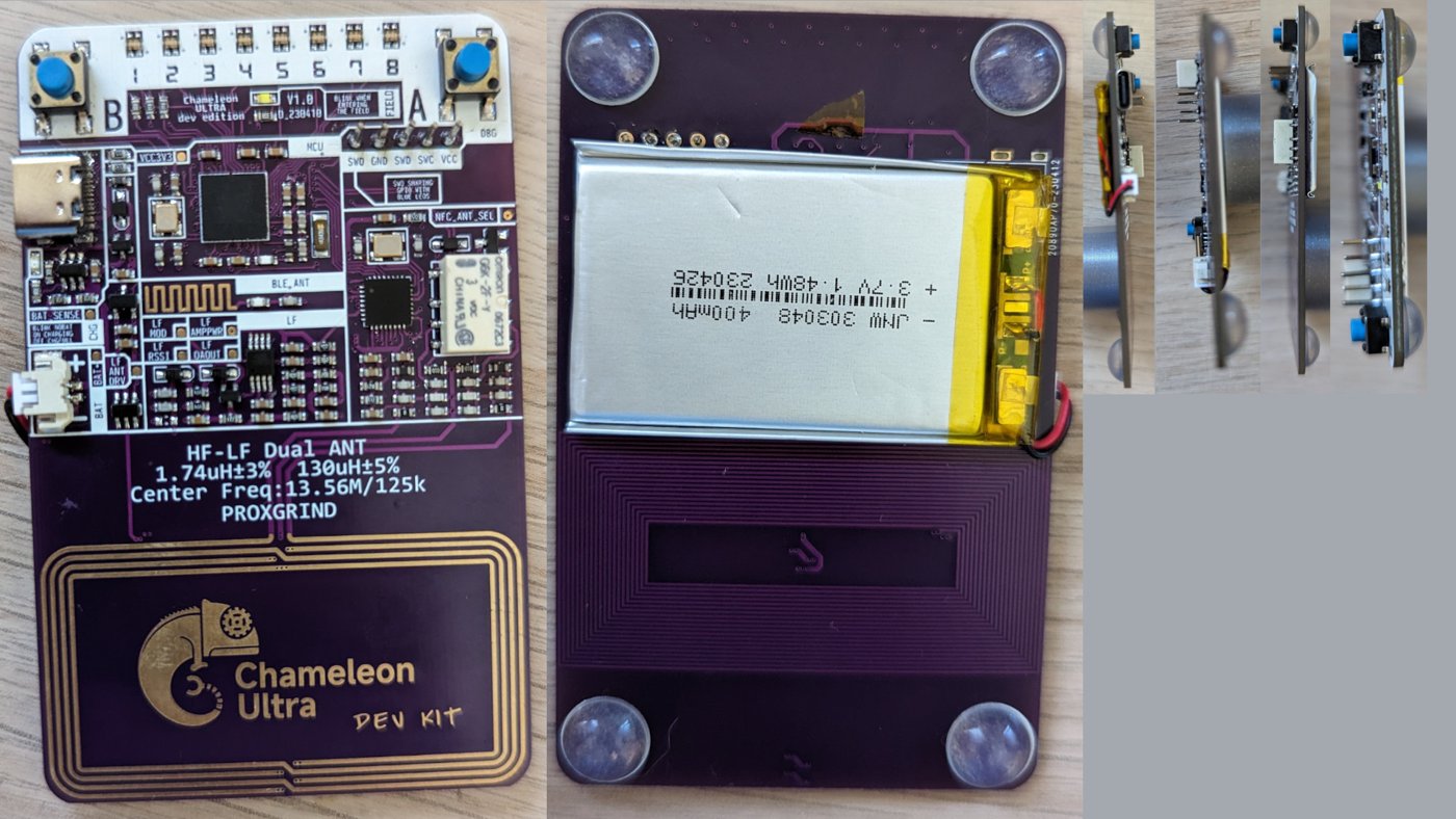
The internal structure is a deliberate three-layer sandwich: a primary PCB carrying the nRF52840, the MFRC522, the HF antenna coil region, all eight RGB-addressed slot LEDs, and the USB-C connector; a passive plastic spacer in the middle housing the 90 mAh LiPo cell and a ferrite pad; and a secondary PCB on the reverse face whose sole purpose is the LF (125 kHz) antenna coil (per the RRG hardware documentation). The ferrite pad in the spacer serves as the isolation layer between the HF coil on the main board and the LF coil on the antenna board — without it, the fields at 13.56 MHz and 125 kHz would partially couple into each other’s coil, degrading both bands’ coupling efficiency. The three-layer assembly is clamped together by thin snap-fit pins rather than screws or adhesive at the PCB stack level; the result is not intended to be field-disassembled, and forcing the housing apart risks snapping the retention pins.
External features visible without disassembly are minimal: two tactile buttons on the face (Button A on the left, Button B on the right), a row of eight RGB LEDs indicating the active slot, a single white LED labeled RF on the edge that illuminates whenever the device detects an RF field on the active slot’s frequency, and the USB-C port recessed in the spacer layer. The gold-on-black PCB aesthetic is visible through the clear back, and the antennas — coplanar traces etched into the antenna board — are identifiable by their spiral geometry.
The rest of this volume works through every component in this assembly at engineering depth: the nRF52840 SoC’s architecture and why it was selected, the MFRC522’s role as the HF reader frontend and the operational consequences of its absence on the Lite, the nRF52840’s peripheral-driven LF path, the antenna geometry of both bands, the LED and button control surface, battery and power management, and the USB-C dual-role port. The Ultra vs. Lite hardware delta gets its own section (§9) since the MFRC522 presence vs. absence is the load-bearing architectural distinction in this product family.
2.2 The nRF52840 SoC
The nRF52840 from Nordic Semiconductor is the Chameleon Ultra’s central compute and RF management platform. Nordic chose to integrate BLE 5.0, an NFC-A tag interface, USB 2.0 Full Speed, and a 64 MHz ARM Cortex-M4F into a single die — a combination that, unusually, gives the Ultra all three of its control paths (BLE, USB, and HF emulation) from one chip. The choice of this specific SoC over simpler alternatives is not accidental: a lesser MCU would force the firmware to offload BLE to a secondary radio module (adding cost, board area, and an inter-chip communication overhead) and would have no path to integrated HF card emulation without yet another RF chip.
2.2.1 Core specs
Table 1 — 2.1 Core specs
| Parameter | Value |
|---|---|
| Core | ARM Cortex-M4 with FPU (M4F) |
| Clock | 64 MHz |
| Flash | 1 MB on-chip |
| RAM | 256 KB on-chip |
| Wireless | BLE 5.0 (2.4 GHz), NFC-A tag interface (13.56 MHz) |
| Wired | USB 2.0 Full Speed (12 Mbit/s) |
| Process node | 55 nm |
| Peripherals | UART, SPI (×4), I²C (×2), PWM (×4), ADC (12-bit), comparators, timers |
The Cortex-M4F’s hardware floating-point unit is less relevant for the Chameleon Ultra’s primary workload — fixed-point Crypto1 LFSR operations don’t need FPU headroom — but the M4F instruction set’s single-cycle multiply, MAC accumulate, and bit-reversal instructions do accelerate the correlation attacks (particularly the parity-bit prediction step in DarkSide and the partial key enumeration in HardNested). The 1 MB of flash comfortably accommodates the GPL-3.0 firmware, the ISO 14443A framing engine, the LF protocol stacks, and the sixteen card-slot storage blocks with room for future protocol additions. The 256 KB of RAM provides enough working space for in-flight MIFARE Classic sector data, the BLE stack’s pairing state, and a complete Crypto1 key-recovery session without requiring external PSRAM.
2.2.2 Role in dual-band operation
The nRF52840 plays two distinct roles in the Chameleon Ultra’s dual-band architecture, and understanding the division of labor is prerequisite to understanding why the MFRC522’s presence or absence defines the Ultra vs. Lite boundary.
For HF (13.56 MHz) card emulation, the nRF52840 uses its integrated NFC-A tag hardware block. This is an on-die analog circuit that can respond to a reader’s 13.56 MHz carrier field, demodulate ASK-modulated commands, and load-modulate a response back — exactly the behavior of a passive ISO 14443A card. When the Chameleon Ultra emulates a MIFARE Classic slot in response to an access-control reader’s anticollision sequence, this is the hardware doing the RF work. The nRF52840’s firmware configures the NFC-A block with the slot’s UID, SAK, ATQA, and sector-key material, and the hardware handles the field interaction from that point. The nRF52840 manages this path in both the Ultra and the Lite.
For LF (125 kHz) operation — both emulation and sniffing — the nRF52840’s general-purpose digital peripherals (PWM, timers, comparators, and GPIO) drive and sense the discrete LF analog front end implemented around the LF antenna coil on the secondary PCB. The nRF52840 generates the 125 kHz carrier via a PWM peripheral, encodes LF protocol modulation in software (Manchester, Biphase, PSK depending on the target protocol family), and demodulates card-present responses through a comparator or ADC input tied to the antenna circuit’s envelope detector. There is no dedicated LF reader IC in the Chameleon Ultra’s bill of materials — the nRF52840’s own peripherals implement the entire LF signal chain. This is why the LF read range is lower than a Proxmark3 RDV4’s dedicated LF path: the Proxmark3 uses a purpose-designed LF analog front end with matched filtering, automatic gain control, and hardware demodulators tuned specifically for 125 kHz; the Ultra’s nRF52840-driven approach trades that fidelity for size and BOM cost.
For HF reading (the MFRC522’s domain), the nRF52840 acts as the SPI master, orchestrating the MFRC522 through the reader-mode command flow: anticollision, select, authentication, and block read. The nRF52840 controls the MFRC522 entirely; the MFRC522 handles the RF-layer mechanics of interrogating a target HF card. This path does not exist on the Lite.
2.2.3 Firmware execution model
The GPL-3.0 firmware running on the nRF52840 is a real-time embedded system structured around a priority-ordered event loop, not a multitasking RTOS in the traditional sense. The firmware manages BLE events, button press processing, USB CDC communication, and the RF event queue (NFC-A tag interactions and MFRC522-initiated reads) from a single execution context with interrupt-driven event staging. The priority ordering ensures that time-critical RF events — particularly NFC-A tag responses, which must meet ISO 14443A timing requirements to the microsecond — are not starved by higher-layer BLE or USB activity. The device enters a low-power sleep state automatically after approximately five seconds of inactivity (no BLE client connected, no USB session active, no button presses), resuming on button press or field detection.
The open-source nature of the full firmware stack means every claimed capability can be verified against the source at RfidResearchGroup/ChameleonUltra, and community contributions regularly add protocol support and attack improvements. The update workflow, community fork landscape, and development environment are covered in depth in Vol 9. From a hardware perspective, the critical implication is that the firmware can be reflashed via the nRF52840’s DFU (Device Firmware Upgrade) bootloader over USB-C without any specialized JTAG/SWD tool — the DFU path is exposed through the same USB-C port used for the CLI.
2.3 The MFRC522 HF reader frontend
The NXP MFRC522 is a mature contactless reader/writer integrated circuit that handles 13.56 MHz RF front-end functions: carrier generation, modulation, demodulation, anticollision, and framing for ISO/IEC 14443 Type A protocols. NXP originally introduced the MFRC522 as a low-cost reader chip for access-control and embedded applications; it is now ubiquitous in hobbyist RFID modules (the common blue RC522 breakout board is built around this chip) as well as production designs. The Chameleon Ultra’s use of the MFRC522 gives it a proven, silicon-validated ISO 14443A reader frontend without the engineering risk of a custom discrete implementation.
2.3.1 What the MFRC522 does
The MFRC522 interfaces to the nRF52840 over a four-wire SPI bus at up to 10 Mbit/s. From the nRF52840’s perspective, the MFRC522 is a peripheral that accepts high-level commands (TransceiveCmd, AuthenticateCmd, etc.) and returns framed card response data; all the RF-layer mechanics are handled inside the MFRC522.
In more detail: the MFRC522 drives a connected antenna coil with a 13.56 MHz carrier, amplitude-key-shift modulates (ASK, 100% or 10% depending on the ISO 14443A bit encoding) the transmit signal for commands, and demodulates the load-modulated subcarrier (848 kHz) in card responses back to bit data. It implements the ISO 14443A anticollision loop in hardware — single-device select, cascade-level UID resolution, SAK validation — and passes the selected PICC’s UID and SAK up to the nRF52840. For MIFARE Classic targets, it executes the three-pass Crypto1 mutual authentication handshake against the nRF52840’s key material, then handles encrypted block read/write operations. Its internal 64-byte FIFO buffers data for both transmit and receive paths, and a flexible interrupt system signals the nRF52840 when transactions complete.
The MFRC522’s modem also supports the higher transfer speeds of the ISO 14443A physical layer: 212 kBd, 424 kBd, and 848 kBd in both directions (versus the base 106 kBd). This is relevant for MIFARE DESFire EV2 and NTAG readers that use faster communication rates.
2.3.2 Ultra vs Lite: the MFRC522 dividing line
The MFRC522’s presence in the Ultra and absence in the Lite defines the most important capability boundary in the Chameleon product family. The distinction is not merely a speed or range difference; it is a fundamental shift in what operations the device can perform.
Without the MFRC522, the Lite has no path to generate a 13.56 MHz carrier field. It cannot interrogate a target card, resolve its anticollision sequence, authenticate to its sectors, or read its memory contents. The Lite’s nRF52840 NFC-A hardware can only respond passively to an incoming reader field — it cannot initiate one. Consequently, a Lite operator in the field must have obtained the card’s UID, sector keys, and memory dump by other means (a Proxmark3 RDV4 session in the lab, a shared dump file, or a ChameleonUltraGUI export from an Ultra-equipped colleague) before loading it into a slot. The Lite is a presentation device, not a capture device.
The Ultra, by contrast, carries out the full read→attack→emulate workflow in a single field session. The MFRC522 reads the target card’s UID and SAK, the nRF52840 executes a Crypto1 attack (DarkSide or Nested being the most common for factory-keyed MIFARE Classic deployments), the recovered sector keys are used to read the full memory dump, and that dump is loaded into a slot — all before the Ultra’s operator has left the vicinity of the target reader. For access-control audits where the goal is validating whether emulated credentials can defeat a reader — without leaving a physical clone behind — the Ultra’s MFRC522-enabled read-in-place workflow is the defining operational advantage.
The MFRC522 is also what enables the Ultra’s Crypto1 attack suite. The attack algorithms (MFKEY32 v2, DarkSide, Nested, StaticNested, HardNested) exploit weaknesses in the MIFARE Classic Crypto1 stream cipher. To mount these attacks, the device must act as a reader: it must send authentication requests, receive the nonce-response pairs that the Crypto1 cipher generates, and feed those pairs to the key-recovery computation running on the nRF52840. All of this requires the MFRC522 to drive the reader field. Without it, these attacks are impossible on-device; the Lite can emulate cards with recovered keys but cannot recover keys itself.
2.4 The LF analog path
The Chameleon Ultra’s 125 kHz LF capability is implemented without a dedicated LF reader IC — a choice that distinguishes it from instruments like the Proxmark3 RDV4 (which uses a purpose-designed LF analog front end with the FPGA managing the low-level baseband) and shapes the realistic performance expectations for LF operation.
2.4.1 Signal generation and detection
The nRF52840 generates the 125 kHz carrier by configuring one of its hardware PWM peripherals to a 50% duty-cycle square wave at that frequency, driving the LF antenna coil through a discrete analog driver stage on the secondary PCB. The driver stage amplifies the nRF52840’s GPIO-level signal to antenna drive current sufficient to establish a reader-class 125 kHz carrier field. Modulation onto the carrier — for writing to writable LF tags such as T5577 — is implemented by the nRF52840 software, encoding the protocol-specific baseband (Manchester-encoded for EM4102, Biphase for HID Prox, etc.) as PWM amplitude modulation or frequency variation depending on the target protocol’s encoding scheme.
Card responses are received through the LF coil itself. A responding card load-modulates the carrier at a subcarrier frequency (typically 2 kHz or 4 kHz depending on the protocol family). The nRF52840 detects this modulation through a comparator or ADC peripheral connected to the receive tap of the LF antenna circuit, with the demodulation and decoding logic running entirely in firmware.
The absence of a discrete LF reader chip imposes practical constraints. Read range on LF is shorter than what a Proxmark3 RDV4 achieves — the Dangerous Things forum community has measured the Ultra’s LF read range at approximately 2 cm or less for typical HID Prox credentials, compared to the Proxmark3 RDV4’s 5–10 cm with its purpose-matched LF antenna board. For sniffing (passively capturing an LF exchange between a reader and a legitimate card by positioning the Ultra nearby), the constraints are similar: proximity must be tighter than a dedicated sniffer because the nRF52840’s frontend is not as sensitive as a properly AGC’d analog chain. Vol 5 covers LF read-range optimization and sniffing placement in operational detail; the reference point for comparison against the Proxmark3 RDV4 is in Vol 8 §9.
2.4.2 Supported LF protocol families
The nRF52840’s LF firmware stack supports the protocol families that account for the overwhelming majority of deployed 125 kHz access-control credentials. Per the RRG firmware documentation, the supported families as of current firmware releases include:
- EM4XX — the EM4100/4102 family, the most widely deployed 125 kHz read-only credential in commodity access control; 64-bit, Manchester-encoded, read-only UID
- T5577 — Atmel/Microchip T5577, the dominant LF writable tag, cloneable to most EM4XX and HID Prox configurations; the Ultra supports both reading and writing T5577 blocks, including T5577 password brute-force
- HID Prox — the dominant proprietary LF format in North American commercial access control; 26-bit and multi-bit variants; Wiegand-encoded over FSK
- Indala — Motorola/HID Indala format; common in older North American enterprise installations; ASK/PSK encoded
- FDX-B — ISO 11785 Full Duplex B, the ISO/IEC standard for animal microchip transponders; 128-bit encoding with CRC-16; relevant in veterinary / agricultural access control
- Paradox — Paradox Security Systems proprietary format, common in mid-range residential and light-commercial alarm and access-control systems
- AWD — AWID/Gallagher format, common in Australasian and Pacific commercial installations
- PAC/Stanley — PAC and Stanley proprietary format, common in UK and European commercial installations
This covers approximately 99% of deployed 125 kHz credentials per the Proxgrind vendor documentation. The T5577 brute-force password attack and UID brute-force are covered in Vol 5, along with the protocol-specific read and emulate workflows for each family above.
2.5 Antennas — HF and LF coils
The Chameleon Ultra’s dual-band antenna architecture is the most physically constrained aspect of the design. Both the 13.56 MHz HF coil and the 125 kHz LF coil must fit within a 40 × 24 mm footprint, must be electromagnetically isolated from each other to prevent mutual coupling from degrading either band’s performance, and must maintain the inductive coupling geometry required by their respective ISO standards while operating from a device that is approximately 4 mm thick on the antenna-board half of the stack.
The solution is the two-PCB split: the HF coil occupies the main electronics board (which also carries the MFRC522 and nRF52840), and the LF coil occupies the dedicated secondary PCB on the back face. The ferrite pad in the plastic spacer between them serves both as a flux concentrator for the HF coil and as a shielding layer to reduce LF field coupling into the HF coil geometry. This allows simultaneous dual-band operation — the firmware can energize both paths concurrently without the LF carrier saturating the HF receive chain.
2.5.1 HF coil
The HF coil at 13.56 MHz is etched as a planar spiral into the main PCB’s copper layers. The coil connects to the MFRC522’s differential TX1/TX2 antenna output pins through the antenna matching network, which is a tuned impedance transformation network (typically an L-network or EMC filter topology with series inductors and shunt capacitors) that transforms the MFRC522’s output impedance into the coil’s resonant impedance at 13.56 MHz. The MFRC522 application note (NXP AN10609) describes the standard matching network topology for PCB antenna designs: the resonant circuit is tuned by the combination of the coil’s self-inductance, the external matching network’s reactive elements, and the parasitic capacitance of the PCB trace routing.
The RRG hardware repository (RfidResearchGroup/ChameleonUltra) contains the Gerber files (Chameleon_nrf52_ultra_ant_V1.0.zip) that define the precise coil geometry — trace width, turn count, inter-turn spacing, and layer allocation within the 4-layer PCB stackup. No public teardown or technical document currently confirms the specific coil dimensions (inductance target, number of turns, trace width in µm) in human-readable form outside those Gerber files. From the physical form factor (24 mm width maximum usable aperture) and the standard MFRC522 matching design practice, the coil area occupies the majority of the board’s 24 × 40 mm face — typical for a credit-card-sized HF reader coil — but exact values are not confirmed from public sources as of 2026-06; see the repository’s hardware folder for the authoritative geometry.
In practical terms, the MFRC522-driven HF coil achieves read ranges of approximately 3–4 cm in reader mode (per community measurements on the Dangerous Things forum) for typical ISO 14443A credentials at nominal read power. Emulation range is determined by the passive NFC-A coupling rather than active drive; proximity to the reader must typically be within 2–3 cm for reliable field coupling in emulation mode.
2.5.2 LF coil
The LF coil at 125 kHz is a larger-footprint spiral occupying the secondary PCB’s available face. At 125 kHz, inductive coupling requires a significantly larger coil inductance than at 13.56 MHz to achieve comparable coupling at any given distance — the Q factor of a resonant LF coil is typically maximized with more turns and larger area than the HF coil. Because the secondary PCB is the same 40 × 24 mm footprint as the main board, the LF coil fills that area, likely with more turns than the HF coil and a larger trace width to reduce DC resistance and maximize antenna Q at 125 kHz.
As with the HF coil, the specific LF coil geometry (turn count, trace width, inductance) is defined in the Gerber files in the hardware repository but has not been published in a human-readable form by RRG or confirmed in any community teardown as of 2026-06. What is confirmed: the LF coil is on the secondary PCB, is attached at least partially by adhesive per the hardware wiki (consistent with the observed need to align it precisely relative to the ferrite pad), and connects to the discrete LF driving circuit implemented around the nRF52840’s GPIO/PWM peripherals on the main board via the PCB-to-PCB interconnect.
The LF coil’s practical limitation relative to a Proxmark3 RDV4 LF antenna board — approximately 2 cm read range vs 5–10 cm — is a consequence of both the smaller coil aperture and the absence of a dedicated LF analog front end with matched filtering and AGC. For field-emulation use cases (presenting an LF credential to a reader), coupling distance matters less than for active reading; most installed LF readers place the coil within 1–2 cm of a presented credential, which falls within the Ultra’s emulation range.
2.6 Button, RGB LED, and status indicators
The Chameleon Ultra’s local user interface is intentionally minimal — two buttons and eight RGB LEDs plus one white LED. There is no display and no keypad. The design philosophy is that a phone running ChameleonUltraGUI is the real control surface; the on-device buttons and LEDs are a minimal fallback for slot cycling and status confirmation when the phone is not in hand.
2.6.1 Button behavior
The Ultra exposes two physical tactile buttons (Button A on the left face, Button B on the right face) with the following default actions per the current RRG firmware:
Table 2 — The Ultra exposes two physical tactile buttons (Button A on the left face, Button B on the right face) with the following default actions per the current RRG firmware
| Action | Result |
|---|---|
| Button A short press | Select previous slot (cycle down) |
| Button B short press | Select next slot (cycle up) |
| Button A long press | Copy detected LF or HF tag UID (Ultra only) |
| Button B long press | Copy detected LF or HF tag UID (Ultra only) |
The slot cycle is circular — pressing past slot 8 in either direction wraps to the opposite end. “Slot” in this context means the combined HF+LF slot entry: a slot can hold an HF card, an LF card, both simultaneously, or neither (empty). The LED strip updates immediately on slot change to reflect the new slot’s content state.
The long-press Copy function is an Ultra-only capability that requires the MFRC522 (for HF) or the LF analog path (for LF) to be active. Holding either button when a compatible field is present instructs the firmware to complete an opportunistic UID read of the detected card and load it into the current slot. This provides a one-button “grab and go” capability without launching the BLE app — though it captures only the UID, not the full memory contents or sector keys, so it is most useful for LF UID-only scenarios (EM4100 read-only fobs) rather than MIFARE Classic attacks.
The button functions are configurable via ChameleonUltraGUI, so an operator can remap long-press to a different action or disable button functions during a session where accidental slot changes would be disruptive.
2.6.2 RGB LED states
The Chameleon Ultra has eight individually addressable RGB LEDs, one per slot, arranged in a horizontal strip across the top face. The current firmware (per ChameleonUltraDocs/firmware.md in the RRG documentation repository, last updated 2025-04) defines the following color-to-state mapping:
Slot content indicator (active slot, field detected):
Table 3 — Slot content indicator (active slot, field detected):
| LED color | State |
|---|---|
| Green | HF (13.56 MHz) card loaded in the active slot and field detected |
| Blue | LF (125 kHz) card loaded in the active slot and field detected |
| Red | Both HF and LF cards loaded in the same slot (dual-configured) |
Note that these colors reflect field interaction — the active-slot LED illuminates in the appropriate color when a reader field is detected and the slot responds. During idle (no field), the slot LEDs reflect the configured content rather than a field event.
Device status indicators:
Table 4 — Device status indicators:
| Pattern | State |
|---|---|
| 4 pulsing green LEDs | USB charging in progress |
| Chasing LEDs (left→right for slots 1–4, right→left for slots 5–8) in slot color | USB/CLI session connected (serial client active) |
| White RF LED (edge indicator) | Reader field detected on the active slot’s frequency |
DFU (Device Firmware Upgrade) mode indicators:
Table 5 — DFU (Device Firmware Upgrade) mode indicators:
| Pattern | State |
|---|---|
| LEDs 4 and 5 alternating green | DFU bootloader idle, waiting for firmware image |
| LEDs 4 and 5 fast-blinking blue | Firmware write in progress (do not disconnect) |
| LEDs 4 and 5 slow-blinking red | DFU error — see firmware documentation |
The DFU mode is entered via the nRF52840’s built-in bootloader; under normal circumstances the device transitions into DFU mode automatically when a firmware update is initiated via ChameleonUltraGUI or the USB CLI. The slow-red error state indicates a failed or interrupted flash; the recommended recovery procedure is documented in Vol 9.
Sleep behavior: The device enters a low-power sleep state approximately five seconds after the last button press, field detection event, BLE activity, or USB session event. The LED strip powers down during sleep. The first button press or field detection wakes the device; the wake latency is low enough that it is not perceptible in normal access-control reader presentation scenarios.
2.7 Battery and power management
The Chameleon Ultra is powered by a 90 mAh lithium polymer (LiPo) cell — a 302020-footprint cell, meaning 3 mm thick × 20 mm × 20 mm, housed in the plastic spacer layer between the two PCBs. The cell is soldered in place; it is not user-replaceable. The 90 mAh capacity is a design point that balances the energy requirements of dual-band RF operation and BLE connectivity against the physical volume budget imposed by the device’s 8 mm total thickness.
2.7.1 LiPo cell specs
Per the RRG technical whitepaper, the nRF52840’s current consumption during HF NFC emulation (tag-emulation mode, NFC-A hardware active) is 5 mA at 3.3 V — a modest load, reflecting the fact that the NFC-A hardware is a passive field interaction that does not require the nRF52840 to actively drive an RF carrier. During Crypto1 key-recovery computation (DarkSide, Nested, or HardNested attacks running on the Cortex-M4F), the whitepaper states 7 mA at 3.3 V for the compute phase. These figures describe the nRF52840’s own current contribution; MFRC522 active reader current and LF driver circuit current are additional draws that are not separately quantified in the currently published RRG documentation.
The 90 mAh cell at 3.3 V holds approximately 297 mWh of usable energy. At 5 mA × 3.3 V = 16.5 mW continuous emulation load, that implies approximately 18 hours of continuous HF emulation before exhaustion — consistent with a device intended for intermittent field use, not 24-hour continuous RF operation. At 7 mA × 3.3 V = 23.1 mW for active Crypto1 computation, the battery budget shrinks to approximately 13 hours of continuous attack computation.
The standby power profile is more important for real-world battery life, since the device spends most of its time waiting rather than actively interrogating cards or running attacks. The nRF52840 enters sleep mode after approximately five seconds of inactivity, during which the Cortex-M4F and most peripherals are suspended and current draw drops to the nRF52840’s System OFF leakage floor — approximately 0.4–0.7 µA per the Nordic nRF52840 Product Specification (the chip-level floor only; real-world system current, including board leakage and regulator quiescent, is typically 1–3 µA in a real design). The MFRC522 in hard POWER_DOWN (NRSTPD pin driven low) draws approximately 10 µA per the NXP MFRC522 datasheet (Rev 3.9). At those levels, the combined sleep current of an nRF52840 in System OFF (~0.5 µA chip floor) plus an MFRC522 in POWER_DOWN (~10 µA) is roughly 10–11 µA at the chip level — comfortably under the ~20 µA budget implied by the Lab401 six-month standby claim. Whether the RRG firmware in fact asserts POWER_DOWN (NRSTPD low) during sleep or uses the MFRC522’s internal soft power-down mode is not explicitly documented in the RRG firmware documentation as of 2026-06; either way, the MFRC522’s POWER_DOWN current of ~10 µA is low enough that the six-month standby budget is achievable without requiring separate supply-gating circuitry to cut power to the chip entirely. Specific measured standby current figures have not been published by RRG or confirmed by community measurement as of 2026-06.
The practical implication: the Chameleon Ultra can be loaded with card slots, carried daily, and presented to readers occasionally without requiring frequent recharging — the six-month standby claim from the vendor matches observed community usage. What it cannot do is run continuous MFRC522 reader-active sessions or sustained Crypto1 attack loops for multiple hours in a single charge; for bench-mode attack work, USB power keeps the device topped up.
2.7.2 Charging behavior
The 90 mAh LiPo cell charges via the USB-C port using a standard lithium-ion CC/CV charging profile. The maximum charge current reported by the community is approximately 50 mA, which gives a full charge time of roughly two hours from flat — appropriate for a device this size and not harmful to a 90 mAh cell at this C-rate (0.55 C). The four-pulsing-green-LED pattern on the slot strip is the charging indicator; when the LED pattern transitions to steady (or off) and the device responds to button presses normally, the charge cycle is complete.
The charge controller is on the main PCB, integrated with the USB-C power delivery circuit. No active battery management display is exposed to the user in the current firmware; there is no fuel gauge peripheral that reports state-of-charge over BLE or USB CLI. Low-battery state does not generate a distinct LED warning in the current firmware — the device will continue to operate until the LiPo’s undervoltage lockout threshold is hit, at which point it will power off without warning. Community users have noted that in practice, the six-month standby characteristic means low-battery surprises in the field are rare for operators who charge the device monthly.
2.8 USB-C interface
The USB-C port on the Chameleon Ultra serves two entirely separate functions over the same connector: power (charging the LiPo cell) and data (the USB 2.0 Full Speed device port of the nRF52840, presenting as a USB CDC ACM serial device for the CLI). Both functions operate simultaneously — the device charges while a CLI session is active, and there is no need to disconnect from a command session to charge.
When the nRF52840’s USB stack enumerates over a connected host, it presents as a virtual serial port (CDC ACM device class). The host OS assigns a COM port (Windows), /dev/ttyACM* (Linux), or /dev/cu.usbmodem* (macOS) entry. The Chameleon Ultra CLI accepts the same command set that ChameleonUltraGUI uses internally over its BLE protocol, with the same slot-management, firmware-management, and RF-operation commands. The USB CLI is the appropriate interface when BLE is not available or desirable — in RF-quiet environments, during firmware update troubleshooting, or on a workstation without a BLE adapter.
The USB connection also triggers the chasing-LED animation on the slot strip (described in §6.2) to visually confirm that a serial session has been established — a useful confirmation when plugging in from a locked workstation where the COM port assignment is not immediately visible.
DFU access over USB uses the nRF52840’s built-in USB DFU bootloader, which exposes a separate USB device (Nordic Semiconductor DFU target) to the host when DFU mode is active. The DFU mode is reached either by issuing the DFU command from the CLI (hw dfu) or from the firmware update dialog in ChameleonUltraGUI. During DFU operation, the standard CLI is not available — the device is entirely in the bootloader. The DFU mode LED pattern (§6.2) distinguishes DFU-idle from DFU-write-in-progress from DFU-error, providing visual confirmation at each stage of the update without requiring a terminal session.
The USB-C connector is recessed into the plastic spacer layer, positioned at the midpoint of the 40 mm edge. This placement is intentional: centered on the spacer layer, it is accessible without a precision-fit cable and allows the device to remain plugged in while lying flat on a bench or in a holder. The standard USB-A-to-USB-C cable included with the device is functional but short; longer cables work without issue given the USB 2.0 Full Speed electrical limits.
Vol 6 covers the CLI command reference for the read/sniff/attack workflow in operational depth; Vol 7 covers the slot-management CLI commands; Vol 9 covers DFU and firmware update procedures.
2.9 The Chameleon Lite — what changes
The Chameleon Lite is the emulation-only member of the RRG/Proxgrind Chameleon family — same firmware lineage, same GPL-3.0 codebase, but with three hardware changes that together define a fundamentally different operational envelope: no MFRC522, a button-cell battery rather than a LiPo, and a larger single-PCB form factor. Understanding the Lite as a hardware delta from the Ultra (not as a lesser version of an otherwise-identical design) clarifies the cases in which it is the correct tool.
2.9.1 Hardware comparison table
Table 6 — 9.1 Hardware comparison table
| Parameter | Chameleon Ultra | Chameleon Lite |
|---|---|---|
| Form factor | 40 × 24 × 8 mm, 8 g | 61 × 36 × 8 mm |
| PCB structure | 2 PCBs + plastic spacer | Single PCB, blue plastic housing |
| MCU | nRF52840, Cortex-M4F @ 64 MHz | nRF52840, Cortex-M4F @ 64 MHz |
| HF reader frontend | MFRC522 (present) | None (absent) |
| HF emulation | Yes (nRF52840 NFC-A hardware) | Yes (nRF52840 NFC-A hardware) |
| LF emulation | Yes (nRF52840 LF path) | Yes (nRF52840 LF path) |
| HF card reading | Yes (MFRC522) | No |
| Crypto1 attacks on device | Yes (MFKEY32 v2, DarkSide, Nested, StaticNested, HardNested) | No |
| Battery | 90 mAh LiPo, USB-C charged | Button cell (35 mAh), USB-C charged |
| Standby life | ~6 months | Longer (lower quiescent draw) |
| HF slots | 8 | 8 |
| LF slots | 8 | 8 |
| Control interface | BLE (ChameleonUltraGUI) + USB-C CLI | BLE (ChameleonUltraGUI) + USB-C CLI |
| Attack capability | Full (read + attack + emulate) | Emulate-only (no live-card read) |
| Price tier | Higher | Lower |
The nRF52840 is identical across both variants; the firmware codebase is shared, with conditional compilation gates for the MFRC522-dependent features (reader commands, attack commands, the Copy UID long-press button action). A Lite running the same firmware build as an Ultra will simply report “reader not available” for any command that requires the MFRC522.
The Lite’s battery is cited in the RRG technical whitepaper as a 35 mAh 10 mm × 40 mm button lithium cell — significantly smaller than the Ultra’s 90 mAh LiPo. Note that the current Lab401 Chameleon Lite product page lists a 90 mAh LiPo cell; this discrepancy likely reflects a hardware revision between the whitepaper’s reference design and the current production unit, but RRG has not published a formal changelog confirming the change. Treat the specific battery type as version-dependent: the 35 mAh figure is correctly sourced from the RRG whitepaper, but production units may differ. Because the Lite has no MFRC522 to power during any operation, and because emulation-only workloads use only the nRF52840 NFC-A passive path (which draws around 5 mA at 3.3 V during field interaction), the Lite’s quiescent and active current draw is lower and the button cell provides adequate runtime for its intended workload despite the smaller capacity.
2.9.2 When to choose the Lite
The Lite is the correct choice when the operator’s workflow is exclusively credential presentation — loading a pre-captured card dump from an external source and emulating it against access-control readers — and when active reading, Crypto1 attacks, or on-device key recovery are never required in the field. Access-control system installers or red-team members who obtain card dumps through other means (Proxmark3 RDV4 in the lab, iCopy-X capture sessions, or shared dump files from a colleague’s Ultra) and need a small, inconspicuous emulator to carry in a card pocket benefit from the Lite’s lower price and simpler workload profile.
The Ultra is the correct choice whenever the field workflow requires reading a card that the operator does not already have a dump of, running Crypto1 attacks to recover unknown sector keys, or carrying out the full read→attack→emulate loop in a single field session. For most physical-pentest and access-control audit engagements — where the operator does not know in advance which cards will be encountered and cannot pre-capture dumps in the lab — the Ultra’s MFRC522 is essential.
The decision rarely comes down to standby life or price when the task scope is clear. Where it does — pure credential presentation at known sites with pre-loaded dumps — the Lite is the more economical and lower-maintenance tool. Operators who might need either capability in the same engagement should carry the Ultra.
2.10 Teardown notes
The Chameleon Ultra is not designed to be field-disassembled. The housing is held together by thin snap-fit retention pins rather than screws, and forcing the case apart risks snapping those pins permanently. The included small screwdriver provides access to the screws that secure the device to its keychain loop (an attachment point at one end of the 40 mm length), but this does not open the device housing itself.
2.10.1 Known teardown resources
The most authoritative source of internal construction information is the RRG hardware wiki and documentation at github.com/RfidResearchGroup/ChameleonUltra/wiki/hardware and the companion ChameleonUltraDocs/hardware.md. These documents were authored by the firmware team and describe the internal architecture from first-party knowledge — the two-PCB-plus-spacer structure, the component placements, the battery type, and the ferrite pad isolation layer are all explicitly documented there. The hardware Gerber files (Chameleon_nrf52_ultra_V1.0.pdf schematics and Chameleon_nrf52_ultra_ant_V1.0.zip antenna Gerbers) in the repository are the authoritative source for PCB-level component placement, coil geometry, and schematic connectivity, though reading them requires EDA tooling (KiCad or equivalent).
Community-level teardown data is sparse. The Dangerous Things Forum review thread for the Chameleon Ultra (forum.dangerousthings.com/t/proxgrind-chameleon-ultra/19756) contains user reviews and operational observations but no physical teardown — the reviewer explicitly declined to open the housing to avoid damaging the silicone case. No Reddit teardown post, YouTube teardown video, or iFixit-style disassembly guide for the Chameleon Ultra was identifiable in public sources as of 2026-06. The device’s fragile snap-fit housing and the general expectation in the RFID community that PCB-level access is not needed for normal operation likely account for this gap.
2.10.2 Notable observations
From the first-party hardware documentation and community operational reports, the following construction facts are confirmed without independent teardown verification:
The two-PCB split with ferrite isolation is confirmed by the RRG hardware wiki. The battery is soldered in place (confirmed by documentation notes about non-replaceability and the housing’s snap-fit-only assembly). The MFRC522’s presence on the Ultra PCB is confirmed by the hardware wiki and the firmware’s conditional compilation structure — the chip is referenced explicitly in both the schematic schematics and the firmware source tree (nrfx_spi peripheral initialized for the MFRC522 interface). The LF antenna is adhesive-attached to the secondary PCB per the hardware wiki; the troubleshooting documentation notes that “glue or resin residues” on the antenna PCB assembly can cause LF coupling issues, implying the LF coil is potted or glued rather than screw-mounted.
No independent teardown with photographs of the internal PCBs, component markings, solder quality, or testpoint locations has been published in accessible form as of 2026-06. Observations about solder workmanship, component branding, testpoint accessibility, or rework difficulty cannot be confirmed from current public sources. Engineers planning to conduct their own teardown for repair or hardware modification should refer to the official schematics in the repository before applying any force to the housing — the two-PCB structure means that the main PCB (carrying the nRF52840 and MFRC522) and the antenna PCB are electrically connected by an inter-board connector that must be separated before either board can be inspected independently.
Comments (0)