Clockwork PicoCalc · Volume 2
PicoCalc Volume 2 — The Carrier Board
ClockworkPi v2.0 Mainboard: Theory of Operation, Schematic Walkthrough, and BOM
Contents
1. Introduction
This volume is the engineer’s reference for the PicoCalc carrier board itself — the ClockworkPi v2.0 mainboard — separate from whichever Pico-shaped compute module happens to be in the socket on a given day. Where Volume 3 covers the modules and Volume 4 covers the bootloader stack, this volume covers the silicon-and-copper underneath: power tree, STM32F103R8T6 keyboard coprocessor, ILI9488 LCD subsystem, AXP2101 PMU, PSRAM, SD I/O, audio, and the side-header break-out.
The full schematic is published by ClockworkPi on GitHub under GPL v3 as clockwork_Mainboard_V2.0_Schematic.pdf1. Page references throughout this volume are to that PDF. Where I had to read the silkscreen on a real unit because the schematic was ambiguous or because a board revision diverged, that is called out explicitly.
The carrier is interesting from a design-review standpoint because it makes a small handful of unusual choices. It uses a single-cell-Li PMIC (AXP2101) on a 2-cell-series battery pack, which works only because of how the cells are wired (more on this in §4). It puts the keyboard on a dedicated MCU rather than scanning the matrix from the Pico — a design decision driven by I²C-slave keyboard semantics rather than I/O scarcity. It runs the LCD on SPI rather than parallel RGB despite using a chip (ILI9488) that supports both — this trade is bandwidth for pin count, and we’ll do the math on it. The audio output is two-channel PWM sharing one timer slice, which is a curious limitation and the source of a perennial forum complaint. None of these are bugs; all are choices with consequences.
1.1 Conventions in this volume
- Net names, designator references, and pin numbers are quoted from the v2.0 schematic. Where I shorten a net name for readability the original is in parentheses on first use.
- “Carrier” or “mainboard” means the ClockworkPi v2.0 PCB. “Module” means the Pico-shaped board in the socket. “STM32” or “keyboard MCU” means the U2 STM32F103R8T6.
- Voltages are nominal unless tolerance is called out. The two cells are nominally 3.7 V each, in series at the battery connector → 7.4 V system rail before regulation, but see §4.4 for what the AXP2101 actually does with that.
- I use “BIOS” only in this volume’s index for cross-reference — see Volume 4 for the keyboard MCU firmware, which the community calls the BIOS.
- All component-count and BOM numbers are observed from the schematic and from disassembled units. Production runs may have undocumented substitutions.
2. Block Diagram and Top-Level Architecture
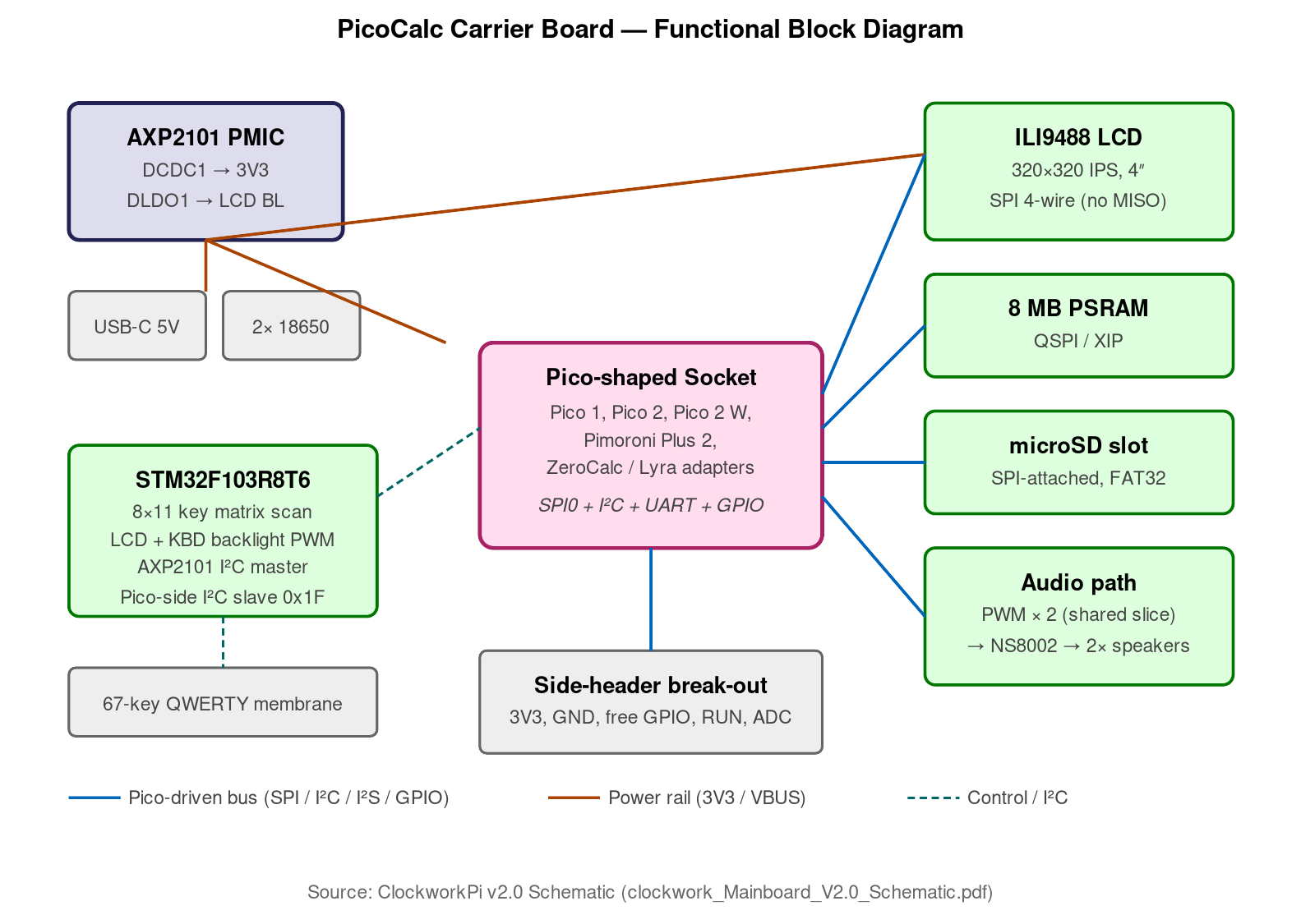
Figure 2.0 — Carrier-board block diagram. Source: ClockworkPi v2.0 Schematic (clockwork_Mainboard_V2.0_Schematic.pdf).
The ClockworkPi v2.0 partitions the device into seven functional blocks, each of which gets its own chapter below:
                    ┌──────────────────────────────────────────────┐
                    │      ClockworkPi v2.0 Carrier Board          │
                    └──────────────────────────────────────────────┘

   USB-C ─── AXP2101 ── 3.3 V system rail ─┬──── Pico module socket
   2× 18650 ──┘  (PMU + charger)           │     (USB pass-through)
                                            │
                                            ├──── STM32F103R8T6 (U2)
                                            │     ├─ key matrix scan
                                            │     ├─ backlight PWM ×2
                                            │     ├─ AXP2101 I²C master
                                            │     └─ I²C slave 0x1F to Pico
                                            │
                                            ├──── ILI9488 LCD module
                                            │     (SPI from Pico, BL via STM32)
                                            │
                                            ├──── 8 MB PSRAM (QSPI/XIP from Pico)
                                            │
                                            ├──── microSD slot
                                            │     (SPI from Pico)
                                            │
                                            ├──── PWM audio (Pico GP26/GP27 → speakers)
                                            │
                                            └──── side-header break-out
                                                  (Pico GPIO + 3.3 V + GND)
The architectural decision worth pausing on: the STM32 owns the keyboard end-to-end, including matrix scan, backlight PWM (both LCD and keyboard), the power button, and the AXP2101’s I²C interface. The Pico talks to the STM32 over a single I²C bus and asks “give me a key event” or “set backlight to N.” This means the Pico cannot reach the keyboard or the PMU directly. The advantage is that the Pico can be hot-swapped or completely reflashed without affecting any of those subsystems; the disadvantage is that a buggy STM32 firmware update can render the entire device useless even if the Pico is fine.
3. Power Tree (AXP2101 PMU)
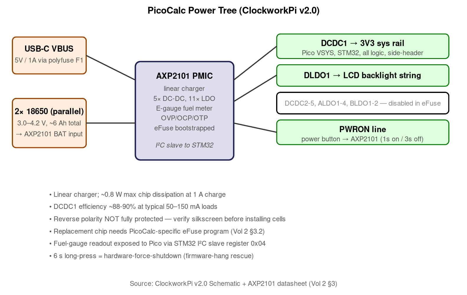
Figure 3.0 — PicoCalc power tree. Source: ClockworkPi v2.0 Schematic + AXP2101 datasheet, §3.
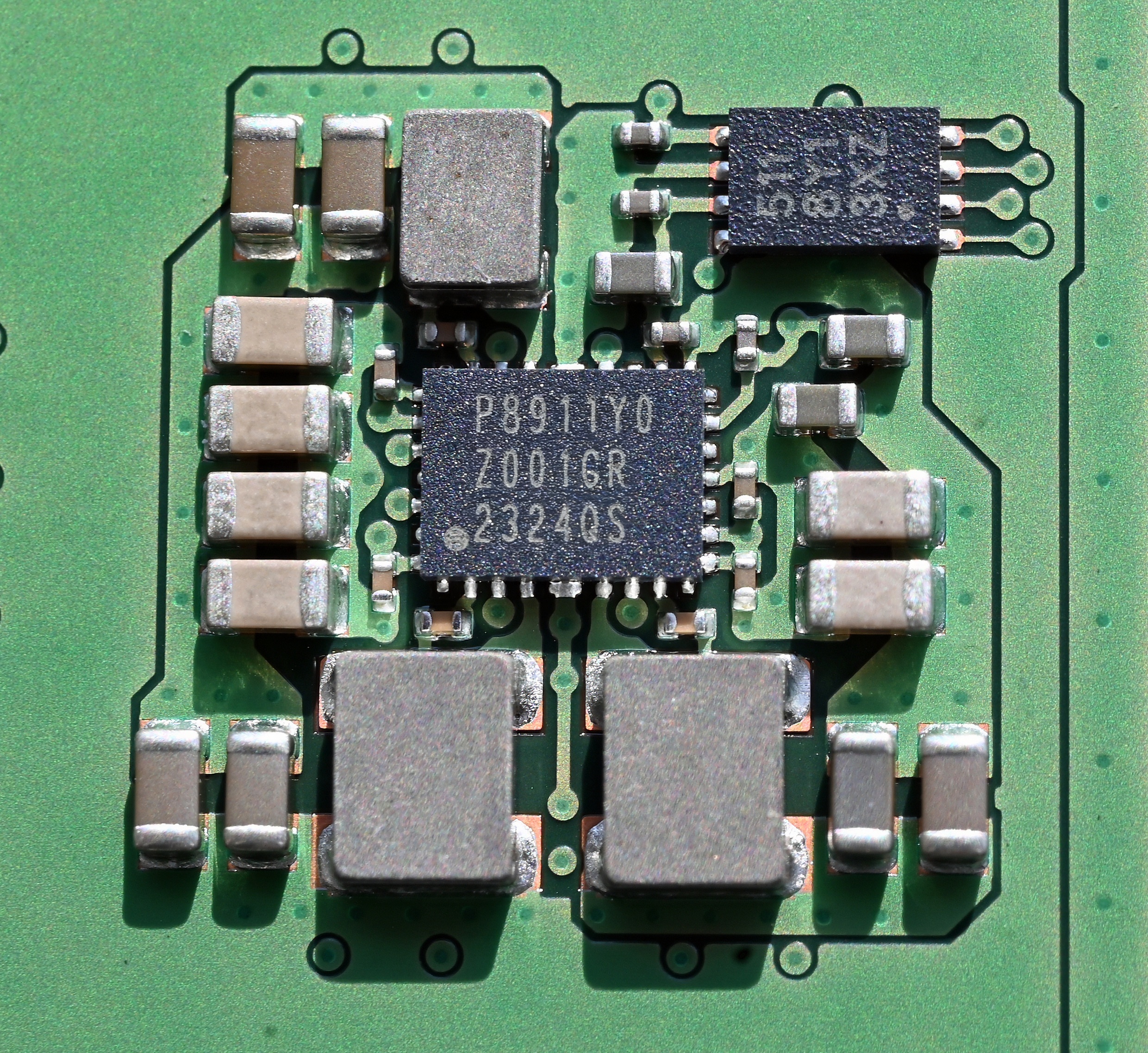
Figure 3.1 — PMIC package reference. File:PMIC chip from Hynix DDR5.jpg by Bubba73. License: CC BY-SA 4.0. Via Wikimedia Commons.
The AXP21012 is the heart of the power subsystem. It is a single-cell Li-battery NVDC (narrow-Vdc) PMIC from X-Powers, integrating a linear charger, five buck DC-DCs, eleven LDOs, an ADC for cell voltage / current / die-temperature, an E-gauge fuel-gauge block, and a small set of GPIO. It is normally specified for 3.0 V – 4.5 V single-cell input.
3.1 The two-cell topology — what’s actually happening
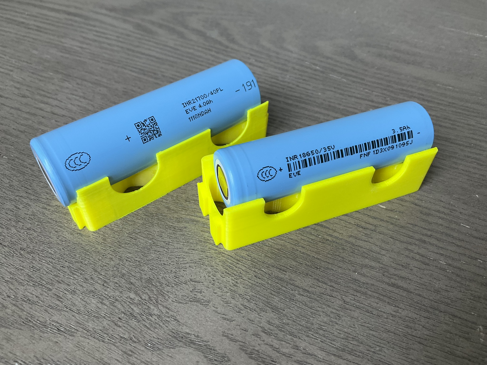
Figure 3.0 — 18650 cells. File:18650 and 21700 lithium ion battery cell.jpg by Sevenethics. License: CC0. Via Wikimedia Commons.
The PicoCalc draws from two 18650 cells. The schematic shows them wired in parallel, not in series — both cells’ positive terminals are tied together at the AXP2101’s BAT input, both negatives to GND. Total capacity at the connector is 6000–7000 mAh at a single-cell voltage (3.0–4.2 V). This is what lets a single-cell PMIC run two cells: from the chip’s perspective there is one big cell.
This has two consequences worth understanding:
- Cell matching matters. With cells in parallel, mismatched internal resistance causes circulating currents. The kit gets away with it because consumer 18650s from the same batch are usually within a few mΩ, but using mismatched cells (different brands, or new + used) is a bad idea — at minimum you lose capacity, at worst you cook the lower-Ri cell.
- Overall current capability is the sum of both cells’ continuous discharge ratings. Two Samsung 35E (8 A continuous each) → 16 A available, far more than the device needs. This is why the PicoCalc tolerates short current spikes (WiFi association on a Pico 2 W can pull 250 mA peak) without browning out.
Some forum posts mention a “series” wiring; that’s wrong. The two cells are parallel. Confirm by reading the schematic, page 1, the BATT_P net.
3.2 The eFuse problem — why a replacement AXP2101 doesn’t drop in
The AXP2101’s default register map is loaded from on-die eFuses at power-on. ClockworkPi’s stock chip ships with a factory eFuse program tailored to the PicoCalc — specifically, the buck and LDO default voltages, the charge termination current, and a small list of register-map edits. A bare AXP2101 from LCSC3 or Mouser will boot with X-Powers’ generic defaults, which do not match what the PicoCalc expects. Symptoms range from “screen comes on but Pico doesn’t boot” to “buck rail oscillates.”
If the AXP2101 ever needs replacement (forum reports a handful of users with reverse-polarity blow-outs, see §3.3), the recovery path is:
- Solder in a new AXP2101.
- Connect the AXP2101’s I²C lines to a host (any USB-I²C dongle works — the Bus Pirate or an Aardvark are convenient).
- Run the eFuse-rewriting script published by ClockworkPi4 on the host. The script writes the PicoCalc-specific register set into the AXP2101’s RAM, then triggers an eFuse program cycle.
- Power-cycle. The new chip now behaves like a stock one.
The eFuse is one-time-programmable in the sense that each fuse bit can be flipped from 0 to 1 only once per chip. The script uses fuses that are still 0 from the factory, so it works on a virgin chip; once burned, the chip is committed.
3.3 Reverse polarity protection — and where it isn’t
The AXP2101 has internal back-to-back FETs on the BAT input that handle short-duration reverse polarity. They survive a brief mis-insertion (long enough to notice “the screen didn’t come on” and pull the cells), but continued reverse polarity will let through enough current to damage the battery-side ESD diode array on the AXP2101. After that the chip is junk — the reverse-protection FETs may still work but the ADC / fuel-gauge / charger will be partially or fully dead.
Forum thread #21627 has photos of the failure mode. Several users report that the LCD backlight comes on after reverse-polarity damage but neither charging nor cell-voltage telemetry works.
The mainboard’s only physical defense is the silkscreen polarity markings around the cell holders. They are not strongly contrasted on early board revisions; later revisions added a bigger + and − on the silkscreen and a directional arrow.
3.4 Output rails
The carrier uses a small subset of the AXP2101’s available outputs:
| AXP2101 output | Voltage | Configured by | Loads |
|---|---|---|---|
| DCDC1 | 3.300 V | eFuse default | Pico VSYS (via socket), STM32 VDD, all logic on the carrier, side-header 3V3 |
| DCDC2 | unused | disabled | — |
| DCDC3 | unused | disabled | — |
| DCDC4 | unused | disabled | — |
| DCDC5 | unused | disabled | — |
| ALDO1–4 | unused | disabled | — |
| BLDO1–2 | unused | disabled | — |
| DLDO1 | 3.300 V | eFuse default | LCD VLED string driver (backlight) |
| DLDO2 | unused | disabled | — |
| CPUSLDO | unused | disabled | — |
DCDC1 carries virtually everything. The buck efficiency at typical PicoCalc loads (50–150 mA) is ~88–90%, which is the dominant power-overhead term in the system battery-life model (Volume 6 has the full thermal-and-power table).
3.5 Charging
Linear charging only — the AXP2101 has no buck-charger. With USB-C input at 5 V and a target of 4.2 V/cell at 1 A charge current, the worst-case dissipation in the chip is (5 − 4.2) × 1 = 0.8 W plus the static current. The QFN-40 thermal pad on the bottom of the chip is the heat path; the carrier’s ground plane under the AXP2101 is solid copper for ~12 mm radius, which gets the chip to about 50 °C die temperature at 1 A charge — within spec but warm enough to feel through the case.
The charge profile is the standard CC/CV: constant-current at the configured rate (default 500 mA, programmable up to 1 A) until the cell reaches 4.2 V, then constant-voltage until current tapers to ~50 mA termination. Total charge time from 3.0 V to full is ~5 hours at 500 mA, ~3 hours at 1 A.
3.6 The fuel gauge
The AXP2101 has a coulomb-counter-based “E-gauge” that integrates current in and out of the cell. After a full charge it knows the cell is at 100%; from there it counts down. It also reads cell voltage and temperature, so if the gauge gets confused (the device sat unpowered for months and self-discharge accumulated), it will re-anchor on the voltage curve.
The gauge is read by the STM32 over I²C, not by the Pico directly. When a Pico stack reports “battery 73%,” it is asking the STM32, which is asking the AXP2101.
3.7 Power-button logic
The power button on the keyboard pad is wired to the AXP2101’s PWRON input, not to the STM32. The AXP2101’s internal logic handles:
- Long-press (~1 s) on a powered-down system → bring up DCDC1 → wake the STM32.
- Long-press (~3 s) on a powered-up system → drop DCDC1 → power off.
- Very-long-press (~6 s, configurable via eFuse) → hardware-force-shutdown regardless of software state. This is the “the firmware is hung” rescue.
The STM32 monitors the same line (via a separate sense) so it can pass short-press events to the Pico over I²C. Long-press handling is purely AXP2101-side.
4. The STM32F103R8T6 Keyboard Coprocessor
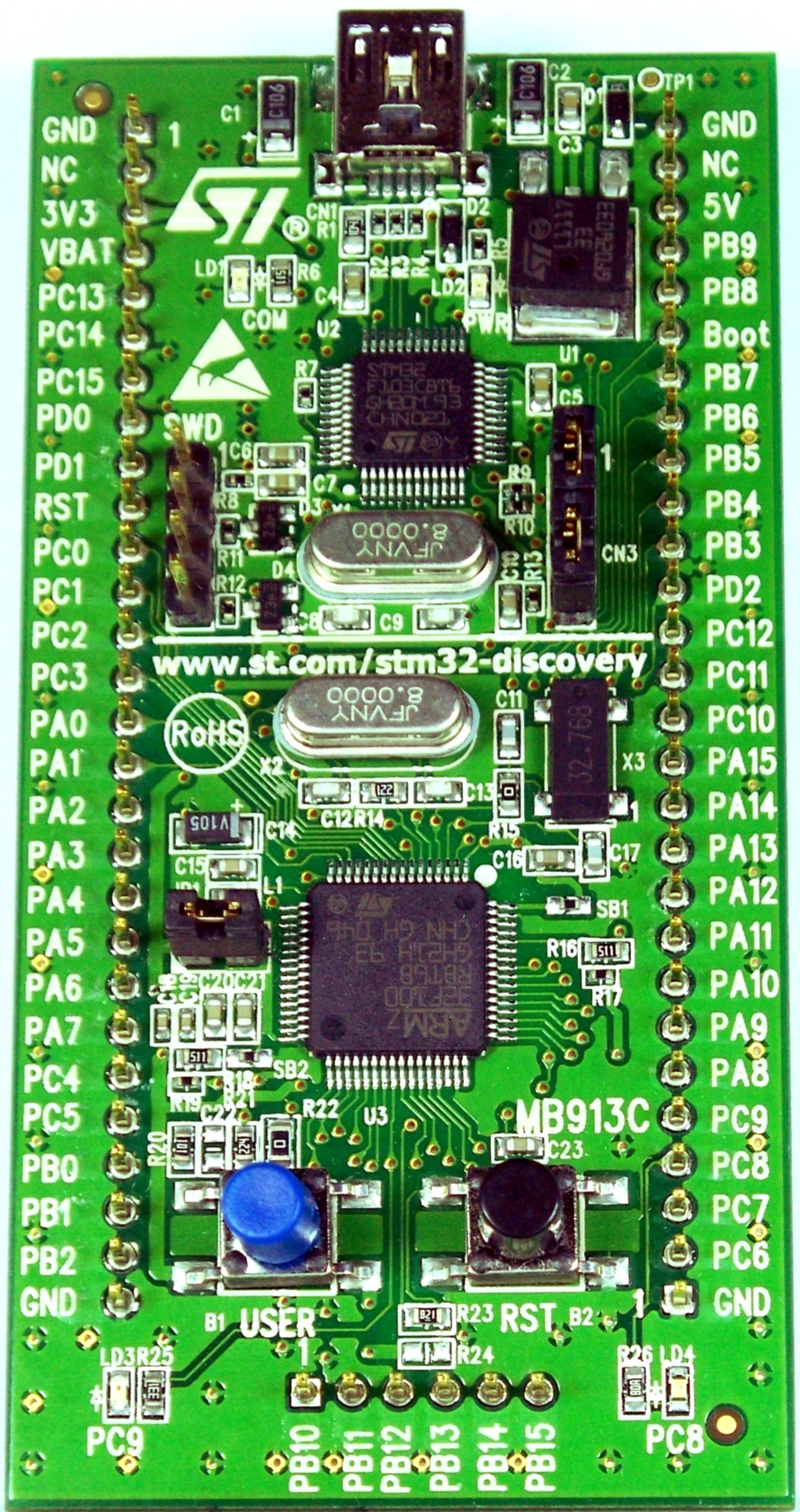
Figure 4.0 — STM32 family LQFP package reference. File:STM32 LV Discovery board.jpg by Viswesr. License: CC BY-SA 3.0. Via Wikimedia Commons (https://commons.wikimedia.org/wiki/File:STM32_LV_Discovery_board.jpg).
U2 on the carrier is an STM32F103R8T65 in LQFP-64 — Cortex-M3 at 72 MHz, 64 KB flash, 20 KB SRAM. The choice of part is a little surprising; an F0-series Cortex-M0 with the same peripheral set would have been adequate and cheaper, but F103s are commodity parts with deep tooling support and the difference is well under a dollar.
4.1 What the firmware actually does
Looking at the source6 (Code/picocalc_keyboard/), the STM32 runs a single super-loop without an RTOS. It services:
- Matrix scan: 8 columns × 11 rows, scanned at ~1 kHz. Columns are driven low one at a time; rows are read with internal pull-ups. Debounce is 8 ms (8 consecutive identical samples).
- Power button monitoring: pin sense for the AXP2101’s
PWRONline. Short presses are translated to keystrokes; long presses are observed but the AXP2101 handles the actual power transition. - LCD backlight PWM: TIM3 channel 1 at ~10 kHz, duty cycle settable from 0–255 over I²C. The LED string is driven through a dedicated FET on the carrier; the STM32 just controls the gate via PWM filtering.
- Keyboard backlight PWM: TIM3 channel 2, same configuration.
- AXP2101 I²C master: STM32 is the I²C master on a private bus to the AXP2101. Polls cell voltage / charge state at ~1 Hz.
- I²C slave to the Pico: STM32 is the I²C slave on the Pico-facing bus, address
0x1F, max bus speed 10 kHz per DeepWiki7. Higher speeds drop events.
4.2 The two I²C busses — keep them straight
It’s easy to confuse the two I²C busses on the carrier:
| Bus | Master | Slave | Speed | Purpose |
|---|---|---|---|---|
| STM32 ↔ AXP2101 | STM32 | AXP2101 | 100 kHz | Power management, fuel gauge |
| Pico ↔ STM32 | Pico | STM32 @ 0x1F | 10 kHz | Key events, backlight commands |
The Pico has no electrical access to the AXP2101 bus. Everything battery-related is mediated through the STM32. This is a deliberate isolation — it protects the AXP2101 from misbehaving Pico firmware, and it lets the STM32 cache battery state so the Pico-side polling rate doesn’t have to be coordinated with the AXP2101’s update rate.
4.3 The I²C slave register map (Pico-facing)
The published register map is small; the most-used registers:
| Reg | Name | R/W | Description |
|---|---|---|---|
| 0x00 | KEY_FIFO | R | Read next key event (returns 0 when empty) |
| 0x01 | FIFO_COUNT | R | Number of pending key events |
| 0x02 | LCD_BL | R/W | LCD backlight 0–255 |
| 0x03 | KBD_BL | R/W | Keyboard backlight 0–255 |
| 0x04 | BATT_PCT | R | Battery percentage 0–100 (from AXP2101 fuel gauge) |
| 0x05 | BATT_MV | R | Battery voltage in mV (16-bit, MSB first) |
| 0x06 | CHARGE_STATE | R | 0=discharging, 1=charging, 2=full |
| 0x07 | FW_VERSION | R | Major.Minor version (1 byte each) |
| 0x10 | RESET | W | Write 0xA5 to soft-reset the STM32 |
Each KEY_FIFO read consumes one event from a circular buffer in the STM32’s RAM. The buffer is 32 entries deep — enough for fast typing without overflow, but a buggy Pico stack that doesn’t drain the FIFO will lose keystrokes.
4.4 The 10 kHz I²C limit
Why 10 kHz when STM32F1’s I²C peripheral is rated to 400 kHz? The STM32 is in slave mode and uses software-driven I²C rather than DMA-driven I²C — the slave-event ISR has to do real work (lookups in the FIFO, register decode) per byte. At 100 kHz the ISR is missing some events; at 10 kHz it has comfortable headroom. The Pico-side drivers (PicoMite, MicroPython, the C SDK keyboard helper) all clock the bus at 10 kHz by default.
If you write your own driver and crank the I²C clock up, expect dropped key events. There is no ACK/NACK feedback that exposes this — the STM32 simply doesn’t see the byte — so debugging it is painful.
4.5 Programming and flashing the STM32
Three independent paths to flash the STM32, covered in Volume 4. Briefly:
- DFU over USB-C: SW107 position 1 routes the STM32’s USB to the case connector, putting the chip into the system-bootloader DFU mode. Use STM32CubeProgrammer.
- SWD via header / test points: SWDIO, SWCLK, GND test points are exposed on the carrier near U2. Use a Pico Probe or any ST-Link clone.
- Bootloader-via-Pico: a community Pico UF2 talks to a running STM32 over the existing I²C bus and pushes a new firmware image. Requires the existing BIOS to be functional.
4.6 The “BIOS 1.4 brick” failure mode, in EE terms
The forum-reported failure mode for v1.4 is that STM32CubeProgrammer aborts with “Operation Exceeds Memory Limits” partway through. What’s happening: the binary file’s specified size is larger than the flash region in the chip variant the programmer is talking to. The STM32F103R8 has 64 KB flash, but some compatible parts (RB, RC) have 128 KB or 256 KB. The 1.4 binary was built against an RB linker script with a 128 KB region, so programmer reports the size mismatch — but partial erase still happened before the abort. The chip ends up with a half-erased flash, no valid reset vector, and won’t boot.
Recovery is straightforward (full-chip erase via SWD, then flash a known-good binary, §4.5). The lesson is that when you build STM32 firmware, link against the actual part variant, and put a STATIC_ASSERT on __app_size__ <= 65536 to catch this at build time.
4.7 Custom firmware — what’s worth changing
The most-common community modifications:
- Keymap: swap to Dvorak / Colemak / AZERTY. The keymap table is a
const uint8_t[8][11]array inkeymap.h. One commit’s worth of work. - Power-button behavior: change long-press timing, add double-tap for screen lock.
- Backlight curve: replace linear PWM with logarithmic to match perceptual brightness.
- Battery telemetry calibration: improve the voltage→percentage curve for specific cell chemistries (NMC vs LFP).
- Add a custom I²C register: e.g., a “deep sleep” command that puts the AXP2101 into hibernate mode while leaving the keyboard MCU awake.
The codebase is small (~3000 lines of C). For someone who’s done STM32 work before, modifying it is a few hours, not days.

Figure 5.0 — IPS LCD module reference. File:LEGEND WITH BOX.jpg by AcumenCam. License: CC BY-SA 4.0. Via Wikimedia Commons.
5. The ILI9488 LCD Subsystem
The display is a 4.0″ 320×320 IPS panel with an integrated ILI9488 driver IC8. The ILI9488 is technically a 320×480 controller; the PicoCalc panel uses its partial-window mode to drive the 320×320 viewable area. SPI 4-wire interface (data + clock + CS + D/C); no parallel-RGB or MIPI-DSI.
5.1 SPI interface and clocking
The Pico drives the LCD on SPI0, with these pins (verify against the carrier silkscreen — minor revision differences exist):
| Pico pin | Net | LCD pin | Function |
|---|---|---|---|
| GP10 | LCD_SCK | SCK | SPI clock |
| GP11 | LCD_MOSI | MOSI | data out |
| GP12 | LCD_DC | D/C | data/cmd select |
| GP13 | LCD_CS | CS | chip select |
| GP14 | LCD_RST | RESET | hard reset |
No MISO — the ILI9488 supports read-back over SPI but the carrier doesn’t wire it. This means you can’t query the display’s status register over SPI; init failures are silent.
Maximum SPI clock: the ILI9488 is rated for 20 MHz write, 10 MHz read (datasheet table 8.7). The Pico’s hardware SPI peripheral can clock to half the system clock, so 62.5 MHz on Pico 1 (125 MHz core), 75 MHz on Pico 2 (150 MHz core). Community drivers run anywhere from 31.25 MHz (conservative, no tearing on any panel revision) to 62.5 MHz (faster but some panels show vertical tearing).
The 62.5 MHz number is over-spec by 3× — the ILI9488 is technically out of compliance. In practice it works on the panels actually shipped with the kit because the trace lengths from Pico to LCD are short (<25 mm) and the LCD’s SPI input has substantial setup-time margin. If you’re writing your own driver, start at 31.25 MHz and only push higher if you confirm clean signals on your unit’s scope.
5.2 Throughput math — why SPI was the right choice
A naive read of “320×320 × 16-bit × 60 fps = 12.3 MB/s” suggests SPI at 31.25 MHz (3.9 MB/s effective after framing) is too slow for 60 fps full-screen redraw. That’s correct. But the workload doesn’t actually demand that:
- Text-mode UIs touch <5% of pixels per frame.
- Full-screen animations are uncommon and can run at 30 fps comfortably.
- True 60 fps full-screen would require parallel-RGB or MIPI-DSI, which would have cost more board area and burned more Pico GPIO than the design budgeted.
So 31.25 MHz SPI gets you ~30 fps full-screen, ~60 fps for partial-screen updates — adequate for the use case, with five Pico GPIO consumed. A parallel-RGB topology would have wanted 16+ pins and a faster MCU. SPI was the right engineering trade.
5.3 Backlight subsystem
The LCD’s LED string is driven from DLDO1 (3.3 V) through a small N-channel MOSFET (Q3 on the schematic) gated by a PWM signal from the STM32 (TIM3_CH1). The PWM frequency is ~10 kHz — high enough to be inaudible but low enough that the FET’s switching losses are negligible.
The PicoCalc reports backlight duty cycle as 0–255 over I²C. 0 is fully off (no current through the LED string); 255 is full brightness (~30 mA continuous through the string). The mapping is currently linear; perceptual brightness is logarithmic, so going from 50% to 100% looks like a much smaller change than going from 5% to 10%. A custom BIOS that applies a gamma curve in the STM32 fixes this.
5.4 Tearing and the TE line
The ILI9488 has a TE (tearing-effect) output pin that pulses at the start of each panel refresh. By gating LCD writes to be aligned with TE, you can avoid mid-frame tearing on full-screen redraws. The carrier does not wire TE. If you cut a trace on the LCD module side and route TE to a free Pico GPIO, you can do vsynced redraws — useful for emulator work where tearing is most visible.
This is the only display-side mod I’d flag as worth doing for graphics-heavy work. It’s a 5-minute solder job (the TE pad is exposed on the LCD’s flex connector at pin 36 on most panel revisions; verify against the supplier’s spec).
5.5 Display ID
The ILI9488 has an internal device ID register (0xD3) that returns 0x00 0x94 0x88 over SPI read. The PicoCalc doesn’t wire MISO, so you cannot read this — the chip identity has to be taken on faith from the schematic and the panel-supplier’s spec sheet. Older docs and forum posts sometimes say “ILI9486” — that’s plausibly correct for an early prototype run, but production units use ILI9488 per ClockworkPi’s BOM.
6. Audio Subsystem
The audio path is the part of the carrier with the most “this is not what I would have done” character. Two PWM channels, both on the same Pico timer slice, driving two speakers through a passive RC filter. The result is “stereo” in name only.
6.1 Routing
The Pico’s GP26 and GP27 leave the socket and run as AUDIO_L / AUDIO_R to two separate RC low-pass networks (R20+C24 and R21+C25 on the schematic), then to a small bridge-tied audio driver IC (a generic NS8002 or equivalent class-AB amp), then to the two speakers via JST connectors.
The two PWM channels share a PWM slice on the Pico (slices 5A and 5B in the RP2040 pin map). PWM slice frequency is shared across both channels — only the duty cycle is independent. So if you set the left channel to 440 Hz and the right channel to 880 Hz, the duty cycles will encode those frequencies but the carrier frequency of the PWM is shared, and aliasing in the RC filter degrades both.
Net effect: it works for chiptune (where both channels are chord-related and aliasing is benign) and beeps. It’s hissy and bandwidth-limited for music or speech.
6.2 The PIO PWM workaround
A community fix uses two of the Pico’s PIO state machines as independent PWM generators, one per channel, freeing them from the shared timer slice. Trade-off: two PIO state machines consumed (you have 8 on Pico 1, 12 on Pico 2 — not a huge deal). Result: actual stereo, modestly better audio quality.
The relevant forum thread9 has working code for both Pico 1 and Pico 2.
6.3 The proper fix — I²S DAC
The clean engineering answer is to bypass the PWM entirely by adding a PCM5102A I²S DAC10 on the side header. Volume 7 has the build instructions; from the carrier-board perspective, the I²S DAC steals three Pico GPIO (GP20/21/22) and outputs analog through its own headphone driver, parallel to or replacing the on-board path.
The PCM5102A has its own integrated 32 Ω headphone amp, so for headphone use you can ignore the on-board NS8002 entirely. For speakers, you still need to drive them — wire the DAC’s analog out into the existing NS8002’s input, or replace the amp.
7. PSRAM Subsystem
The carrier carries an 8 MB PSRAM chip (a Lyontek LY68L640011 or similar — APS6404L is also seen on some board revisions) accessible from the Pico over QSPI. The chip’s CE# is wired to a Pico GPIO that doesn’t conflict with the boot flash; on Pico 1 this is GP0 by convention, on Pico 2 it can be either GP0 or the dedicated PSRAM CS pin.
7.1 Pico 1 vs Pico 2 PSRAM access
Pico 1 (RP2040): PSRAM is accessed through the same QSPI interface as the boot flash, time-multiplexed via software. Performance is limited because every PSRAM access has to swap the QSPI controller’s state and re-enable XIP for code fetches. Realistic burst throughput: ~2 MB/s.
Pico 2 (RP2350): a dedicated PSRAM bus and cache. PSRAM and flash can be active simultaneously. Burst throughput: ~25 MB/s. This is one of the practical reasons Pico 2 is so much better for graphics-heavy work — it can use the carrier’s PSRAM as a frame buffer without giving up flash XIP speed.
7.2 Coexistence with on-module PSRAM
If the module in the socket already has its own PSRAM (Pimoroni Pico Plus 2 has 8 MB on-module), then there are two PSRAM chips active simultaneously:
- The module’s PSRAM, on the module’s own QSPI bus (or dedicated PSRAM bus on RP2350-based modules).
- The carrier’s PSRAM, on the socket-shared QSPI bus.
These don’t interfere as long as the chip-selects don’t collide, but most software targets one or the other, not both. The Pimoroni’s PSRAM gets used by the Pimoroni-aware SDK; the carrier’s PSRAM gets used by PicoCalc-aware code. Coordinating them is an exercise.
8. SD Card Subsystem
The SD slot is SPI-attached to the Pico, not SDIO. SPI signals: CLK on GP10, MOSI on GP11, MISO on GP12 (different from the LCD’s SPI by virtue of different chip-select lines), CS on a dedicated GPIO. The SD card detect line is wired to a free GPIO so software can detect insert / remove.
8.1 SPI-only — performance ceiling
SPI mode on SD is limited to about 25 MHz reliably (the SD card spec allows up to 50 MHz but card-to-card variance is wide). At 25 MHz with 8-bit framing, you get ~3 MB/s sustained read — adequate for streaming UF2s into flash, fine for FAT32 file I/O, slow for video or large datasets.
If the design had used SDIO (4-bit data + clock at 50 MHz), throughput would be ~20 MB/s. The Pico’s PIO can implement SDIO in software; some community drivers do this on RP2350. But the carrier’s SD slot is wired SPI-only — GP9 is wired to CS, no DAT1/2/3 pins available.
8.2 Card compatibility
FAT32 only (the bootloader and most stacks build petit-FatFs without exFAT support). Cards 64+ GB ship pre-formatted exFAT and must be reformatted before first use. Cards larger than 256 GB sometimes have controller quirks that don’t play well with the Pico’s SPI driver — see Volume 4 for the compatibility list.
8.3 Layout — partition vs raw tail
The factory SD layout is a single FAT32 partition occupying almost the full card, with a 32 MB raw partition at the tail. The raw partition is the FUZIX root filesystem — petit-FatFs doesn’t see it (it’s outside the FAT). This is why blowing away the partition table and reformatting kills FUZIX without warning.
If you want FUZIX, you have to recreate the raw partition manually: dd if=fuzix-root.img of=/dev/sdX seek=$((CARDSIZE-32)) bs=1M.
9. USB-C Routing
The USB-C port on the case carries 5 V (charging) and USB 2.0 data. The 5 V routes through a polyfuse (F1, ~1 A trip) to the AXP2101’s VBUS input. The data lines (D+ / D−) route to the Pico’s USB pins through the socket — not to the STM32, except when SW107 position 1 is in DFU mode.
9.1 SW107 — the DFU multiplexer
SW107 is a 4-position DIP switch on the carrier. Position 1 controls a bus multiplexer that routes the case’s USB D+/D− to either:
- Position 1 OFF: USB → Pico (the normal state).
- Position 1 ON: USB → STM32 (DFU mode for keyboard firmware updates).
Positions 2–4 are reserved for future board revisions; on v2.0 they are not connected.
The multiplexer chip (a TS3USB221 or pin-compatible) has effectively zero impact on USB signal integrity at full-speed (12 Mbps) — it adds a few hundred ps of skew and ~5 pF of capacitance, neither of which matters at this rate.
9.2 USB-C VCONN and Power Delivery
The PicoCalc’s USB-C is standard USB 2.0 with no PD negotiation. It pulls 5 V at up to 1 A through the polyfuse; CC1 and CC2 are pulled down with 5.1 kΩ pulldowns to indicate “I am a UFP, give me 5 V default.” It will not charge faster than 1 A even from a 100 W PD charger.
This is fine — 1 A linear charging at 5 V is plenty for two 18650s in parallel. PD support would have added complexity and a separate IC (TPS65987DDH, FUSB302, etc.) for negligible gain.
10. Side-Header Break-out
The side-header is a 2.54 mm pitch dual-row header on the right edge of the carrier, exposing:
- 3.3 V (DCDC1)
- VBUS (USB 5 V passthrough)
- GND (multiple pins)
- Most of the Pico’s free GPIO (those not consumed by LCD, SD, audio, or I²C-to-STM32)
- The Pico’s RUN line (active-low reset)
10.1 Pinout — and the silkscreen vs schematic problem
DigitalDreams’ forum thread #1745612 has a corrected pinout because the silkscreen on early board revisions disagrees with the schematic on a few pins. Trust the silkscreen on your physical unit, not the schematic, not this document, not DigitalDreams’ diagram. Verify with a multimeter before connecting anything.
The most common discrepancies between schematic and silkscreen are the I²S pins (sometimes labeled GP20/21/22, sometimes GP21/22/26 depending on revision) and the secondary I²C pins.
10.2 Signal integrity considerations
The side-header is unbuffered — every pin connects directly to the Pico’s GPIO via a short trace and a pull-up resistor footprint (most are unpopulated). For most uses (LEDs, slow I²C, sensors) this is fine. For higher-speed signals (SPI > 10 MHz, I²S, or anything with sharp edges) the trace length to the header (~30 mm) and the lack of impedance matching can cause ringing.
Practical guidance:
- Slow signals (I²C up to 400 kHz, GPIO toggling at < 1 MHz): no special care needed.
- Medium-speed (SPI to 25 MHz, I²S at 64 fs): add 22 Ω series resistors at the Pico end of the trace if you can. This dampens ringing.
- High-speed (SPI > 25 MHz, anything with < 1 ns rise time): consider routing through a small breakout that has impedance-controlled traces. This is a real concern if you put a high-speed ADC on the side header.
10.3 Mechanical — the cutout
The side-header cutout in the case is sized for headers that stand ≤6 mm above the carrier. Add-on modules taller than that won’t fit with the case closed. The Lyra adapter PCBs (Volume 9) are designed to fit; aftermarket ESP32 modules often don’t. If you need extra clearance, a 3D-printed back from Volume 3 §3.5 or Volume 7 has variants with raised cutouts.
11. Carrier Board Revisions
ClockworkPi has revised the v2.0 board at least twice during the kit’s production run. Differences are small but real:
| Revision | Date | Changes |
|---|---|---|
| v2.0 r1 | Late 2024 | Original release |
| v2.0 r2 | Mid 2025 | Stronger silkscreen polarity markings on cells; minor pad cleanup near AXP2101 |
| v2.0 r3 | 2026-Q1 | Side-header pinout adjusted (added 3V3 sense pin, reordered I²S pins) |
You can identify the revision by reading the small text on the bottom side of the board near the SD slot — it will read CWPI MAINBOARD V2.0 R<n>.
The schematic PDF on GitHub corresponds to v2.0 r1 as of this writing. ClockworkPi has not historically pushed updated schematics for minor revisions — to confirm a specific net on r2 or r3, trace it on a real board.
12. BOM Analysis
The carrier-board BOM is well-suited to small-scale lab reproduction. Most parts are commodity:
| Designator | Part | Package | Notes / source |
|---|---|---|---|
| U1 | Raspberry Pi Pico (socketed) | DIP-40 | not on the BOM — user-supplied |
| U2 | STM32F103R8T6 | LQFP-64 | Mouser ~$5 qty 10 |
| U3 | AXP2101 | QFN-40, 4×4 mm | LCSC C3036461 ~$1.50 qty 10. Requires eFuse program (§3.2) |
| U4 | LY68L6400 / APS6404L | SOIC-8 / WSON-8 | LCSC C2839005 ~$1 qty 10 |
| U5 | NS8002 audio amp | SOP-8 | LCSC C7592 ~$0.30 |
| U6 | TS3USB221 USB mux | TSSOP-10 | Mouser ~$1 |
| LCD | 4″ 320×320 IPS w/ ILI9488 | flex/connector | Multiple suppliers; ClockworkPi-spec part |
| SD | microSD slot (push-push) | molex 502774-0891 | Mouser, 10/$5 |
| Q3 | AO3400 N-FET (LCD backlight) | SOT-23 | Generic; LCSC ~$0.05 |
| Q4–Q8 | various small-signal NPN/NFETs | SOT-23 | Generic |
| Y1 | 8 MHz crystal | 5×3.2 mm SMD | Generic |
| Y2 | 32.768 kHz crystal (RTC) | 3.2×1.5 mm SMD | Generic |
| L1 | 4.7 µH inductor (DCDC1) | 0805 | Coilcraft XAL5050; LCSC alternates |
| C1–CN | 0603/0805 ceramics | 0603/0805 | Generic; X7R 10V |
| R1–RN | 0603 chip resistors | 0603 | Generic |
| F1 | polyfuse, 1 A trip | 1812 | Mouser; Bourns or Littelfuse |
Total active parts: ~12 unique. Total BOM: ~80 placements (resistors, caps, inductors). At 100-unit scale the BOM is well under $30 in parts; the ClockworkPi sticker price of $75 is dominated by the case, the LCD, the keyboard mechanical assembly, and the kit’s curated SD card.
For lab reproduction:
- The schematic and a partial BOM are public1. Gerbers and a placement file are not — those would have to be reconstructed from the schematic and a clear photo of both sides of the board, or from the GPL’d CAD source if ClockworkPi releases it.
- The AXP2101 eFuse step (§3.2) is the gating item if you reproduce the board. Without that, the chip won’t work at the right voltages.
- The LCD is the single hardest part to source — ClockworkPi appears to have sourced it custom or in a small run. Generic 4″ 320×320 IPS panels with ILI9488 are available on AliExpress but pinout varies.
13. Schematic Walkthrough
The published v2.0 schematic1 is 12 pages. Quick guide:
| Page | Title | What’s on it |
|---|---|---|
| 1 | Title block / revision history | Document metadata |
| 2 | Power tree | AXP2101, USB-C input, polyfuse, output filtering |
| 3 | Pico module socket | Pico pin breakout, decoupling |
| 4 | STM32F103 keyboard MCU | STM32 + crystal + decoupling + I²C buses |
| 5 | Key matrix | 8×11 matrix, column drives, row pull-ups |
| 6 | LCD interface | SPI buffers, backlight FET, connector |
| 7 | SD card | SD slot, level shifters, decoupling |
| 8 | PSRAM | LY68L6400 + decoupling |
| 9 | Audio | PWM RC filters, NS8002, speaker connectors |
| 10 | USB-C / DFU mux | USB-C connector, TS3USB221, SW107 |
| 11 | Side-header break-out | All header pins to Pico GPIO |
| 12 | Mechanical | Mounting holes, fiducials, board outline notes |
Worth opening in parallel with this document for cross-reference. Page 2 (power tree) is the most-useful page for understanding battery and PMIC behavior; page 4 (STM32) for understanding keyboard firmware.
14. Common Failure Modes and Repair
14.1 Reverse-polarity AXP2101 damage
Symptom: backlight comes on, Pico boots, but charging doesn’t work and battery percentage reads 0% always. Cause: reverse-polarity insertion of a cell, even briefly. Fix: replace AXP2101, re-program eFuse (§3.2). Difficulty: needs hot air, fine soldering, and a USB-I²C dongle. Time: ~2 hours.
14.2 Cracked LCD ribbon
Symptom: LCD doesn’t init or shows garbage. Cause: ribbon flexed too sharply during disassembly. Fix: replace LCD module assembly. ClockworkPi sells the LCD assembly separately ($25-ish).
14.3 SD slot wear
Symptom: SD insert detection unreliable. Cause: card-detect spring fatigue after many insertions. Fix: replace the SD slot. The Molex 502774-0891 is a drop-in replacement.
14.4 STM32 crystal start-up failure
Symptom: STM32 firmware update succeeds but keyboard never initializes. Cause: crystal Y1 not oscillating (cracked or dead). Fix: replace Y1 (8 MHz, 5×3.2 mm SMD, 18 pF load capacitance). Common failure on units that have been dropped.
14.5 Speaker failure
Symptom: one or both speakers silent. Cause: speaker coil broken or the JST connector is loose. Fix: re-seat the JST first; replace the speaker if that doesn’t work. ClockworkPi-spec speakers are 8 Ω, 0.5 W, 14 mm.
15. Modifying the Carrier — Common Mods
15.1 Adding an external SMA connector for an on-module wireless antenna
If your Pico module is a Pico 2 W and you want better RF range, the on-module CYW43439 antenna is suboptimal inside the metal-coated ABS case. Drilling a small hole in the case and wiring a U.FL-to-SMA pigtail to the module’s U.FL pad (some Pico W revisions populate this; some don’t — check yours) routes the antenna outside the case. Improvement: typically +6 dB on RX, +3-4 dB on TX.
15.2 Replacing the LCD with a higher-DPI panel
Some users have replaced the 4″ 320×320 with a 4″ 480×480 IPS using the same ILI9488 driver. The driver supports it (it’s a 320×480 chip — using more of its native area). The panel mechanical dimensions and ribbon pinout match. Software side: change the LCD init sequence to MADCTL = 0x40 and adjust frame buffer to 480×480 (= 460,800 bytes — needs Pico 2’s PSRAM or stripe rendering). Effective DPI jumps from 113 to 170. Worth doing if you have a Pico 2 in the socket.
15.3 Adding a hardware reset button
The Pico’s RUN pin is exposed on the side header. Adding a small momentary tactile across RUN-to-GND gives you a hardware reset button without opening the case — useful for development.
15.4 Adding a battery pack passthrough
A two-pin JST-PH on the side header wired to BATT_P and GND lets you power the device from an external pack (a 4-cell 18650 power-bank, for example) without using the internal cells. Useful for extended-run field work.
16. Resources
The clickable table below collects every URL referenced in this volume, plus a few extras useful for hardware-level work.
16.1 Primary sources
| Resource | Link |
|---|---|
| ClockworkPi v2.0 schematic | https://github.com/clockworkpi/PicoCalc/blob/master/clockwork_Mainboard_V2.0_Schematic.pdf |
| ClockworkPi PicoCalc GitHub | https://github.com/clockworkpi/PicoCalc |
| PicoCalc product page | https://www.clockworkpi.com/picocalc |
| PicoCalc DeepWiki overview | https://deepwiki.com/clockworkpi/PicoCalc |
| Keyboard subsystem (DeepWiki) | https://deepwiki.com/clockworkpi/PicoCalc/3-keyboard-subsystem |
| Keyboard firmware source | https://github.com/clockworkpi/PicoCalc/tree/master/Code/picocalc_keyboard |
| Arduino setup for keyboard dev (wiki) | https://github.com/clockworkpi/PicoCalc/wiki/Setting-Up-Arduino-Development-for-PicoCalc-keyboard |
| ClockworkPi forum (PicoCalc) | https://forum.clockworkpi.com/c/picocalc/ |
16.2 Component datasheets
| Component | Datasheet |
|---|---|
| AXP2101 PMU | https://files.waveshare.com/wiki/common/X-power-AXP2101_SWcharge_V1.0.pdf |
| STM32F103R8T6 | https://www.st.com/en/microcontrollers-microprocessors/stm32f103r8.html |
| ILI9488 LCD driver | https://www.displayfuture.com/Display/datasheet/controller/ILI9488.pdf |
| LY68L6400 PSRAM | http://www.lyontek.com/upload/products/file/202103080100039_71.pdf |
| APS6404L PSRAM (alternate) | https://www.mouser.com/datasheet/2/1127/APS6404L_3SQR_3SQN-1828594.pdf |
| TS3USB221 USB mux | https://www.ti.com/lit/ds/symlink/ts3usb221.pdf |
| NS8002 audio amp | https://www.ns3000.com/datasheets/NS8002.pdf |
| PCM5102A I²S DAC | https://www.ti.com/lit/ds/symlink/pcm5102a.pdf |
| RP2040 | https://datasheets.raspberrypi.com/rp2040/rp2040-datasheet.pdf |
| RP2350 | https://datasheets.raspberrypi.com/rp2350/rp2350-datasheet.pdf |
| Pico (board) | https://datasheets.raspberrypi.com/pico/pico-datasheet.pdf |
| Pico 2 (board) | https://datasheets.raspberrypi.com/pico2/pico-2-datasheet.pdf |
16.3 Forum threads (carrier-specific)
| Topic | Link |
|---|---|
| AXP2101 eFuse configuration after replacement | https://forum.clockworkpi.com/t/axp2101-pmu-efuse-configuration-after-replacement-help-needed/21627 |
| Side-header pinout (DigitalDreams, corrected) | https://forum.clockworkpi.com/t/picocalc-side-header-pinout/17456 |
| Audio with PIO PWM workaround | https://forum.clockworkpi.com/t/audio-with-pio-pwm/18339 |
| New Keyboard BIOS 1.4 (and the brick story) | https://forum.clockworkpi.com/t/new-keyboard-bios-1-4/19258 |
| Custom PicoCalc BIOS / keyboard firmware | https://forum.clockworkpi.com/t/custom-picocalc-bios-keyboard-firmware/17292 |
| Flashing the latest keyboard firmware | https://forum.clockworkpi.com/t/flashing-the-latest-keyboard-firmware/17240 |
| 3D-printable case bottoms | https://forum.clockworkpi.com/t/3d-printing-models-available/16358 |
| Reverse-engineered case back | https://forum.clockworkpi.com/t/reverse-engineered-case-back-for-the-picocalc/18269 |
| FUZIX on PicoCalc (search the forum for current threads) | https://forum.clockworkpi.com/c/picocalc/?q=fuzix |
16.4 Suppliers (parts and tools)
| Supplier | Link | Notes |
|---|---|---|
| LCSC | https://www.lcsc.com/ | Best for AXP2101, PSRAM, generic discretes. China-shipped. |
| Mouser | https://www.mouser.com/ | Best for STM32, RP-class chips, Coilcraft inductors |
| Digi-Key | https://www.digikey.com/ | Same general class as Mouser |
| Adafruit | https://www.adafruit.com/ | Convenience modules (Pico breakouts, ESP32 boards, sensor breakouts) |
| Pimoroni | https://shop.pimoroni.com/ | Pico Plus 2 modules; PicoCalc-compatible boards |
| Waveshare | https://www.waveshare.com/ | Cheap Pico clones, displays, sensors |
| 18650 Battery Store | https://www.18650batterystore.com/ | Reliable source for Samsung 35E, 30Q; not Amazon |
| Illumn | https://illumn.com/ | Same; flat-top and button-top |
16.5 Tooling for STM32 work
| Tool | Link |
|---|---|
| STM32CubeProgrammer | https://www.st.com/en/development-tools/stm32cubeprog.html |
| STM32duino board package | https://github.com/stm32duino/Arduino_Core_STM32 |
| Raspberry Pi Debug Probe | https://www.raspberrypi.com/products/debug-probe/ |
| OpenOCD (RP2040/RP2350) | https://github.com/raspberrypi/openocd |
17. Index
| Topic | Section |
|---|---|
| AXP2101 — eFuse | §3.2 |
| AXP2101 — fuel gauge | §3.6 |
| AXP2101 — output rails | §3.4 |
| AXP2101 — power-button logic | §3.7 |
Footnotes
-
https://github.com/clockworkpi/PicoCalc/blob/master/clockwork_Mainboard_V2.0_Schematic.pdf. PDF, ~12 pages. The same repository hosts the keyboard firmware source, mechanical files, and 3D-print STLs. ↩ ↩2 ↩3
-
AXP2101 datasheet: https://files.waveshare.com/wiki/common/X-power-AXP2101_SWcharge_V1.0.pdf. The chip is a successor to the AXP202/AXP173/AXP192 family — same vendor, similar register map, much better efficiency and a more complete fuel-gauge. ↩
-
AXP2101 at LCSC: https://www.lcsc.com/product-detail/C3036461.html. ~$1.50 each at qty 10. The chip is a QFN-40, 4×4 mm, 0.4 mm pitch — reflow-only in practice. ↩
-
AXP2101 eFuse recovery thread: https://forum.clockworkpi.com/t/axp2101-pmu-efuse-configuration-after-replacement-help-needed/21627. The script is in the same thread as an attachment. ↩
-
STM32F103R8T6 datasheet: https://www.st.com/en/microcontrollers-microprocessors/stm32f103r8.html. Datasheet
DS5319. Available from Mouser at ~$5/qty 10. ↩ -
Keyboard firmware source: https://github.com/clockworkpi/PicoCalc/tree/master/Code/picocalc_keyboard. Build with the Arduino IDE + STM32duino board package. ↩
-
PicoCalc keyboard subsystem on DeepWiki: https://deepwiki.com/clockworkpi/PicoCalc/3-keyboard-subsystem. Documents the I²C register map and command set. ↩
-
ILI9488 datasheet: https://www.displayfuture.com/Display/datasheet/controller/ILI9488.pdf. 320×480 16.7M-color RGB driver IC, supports 8/9/16/18-bit parallel and 3/4-wire SPI. ↩
-
PIO PWM stereo audio thread: https://forum.clockworkpi.com/t/audio-with-pio-pwm/18339. ↩
-
TI PCM5102A datasheet: https://www.ti.com/lit/ds/symlink/pcm5102a.pdf. 32-bit / 384 kHz I²S audio DAC, $3 in single-board form on AliExpress. ↩
-
LY68L6400 datasheet: http://www.lyontek.com/upload/products/file/202103080100039_71.pdf. 64 Mbit (8 MB) QSPI PSRAM, 33 MHz QPI mode, 1.8/3.3 V. ↩
-
DigitalDreams’ side-header pinout thread: https://forum.clockworkpi.com/t/picocalc-side-header-pinout/17456. ↩