Clockwork PicoCalc · Volume 7
PicoCalc Volume 7 — Add-on Hardware & DIY Boards
Side-header accessories, adapter PCBs from scratch, and where to buy premade
Contents
1. Introduction
This volume is the engineer’s reference for everything that plugs into, attaches to, or replaces the carrier-board hardware. It treats the side-header as a real electrical resource (Volume 2 §10 covered it briefly; this volume goes deeper), walks through the design of the most-useful add-on accessory boards at schematic-and-layout level, and gives the same treatment to the Pi Zero and Lyra adapter PCBs that turn the PicoCalc into a Linux machine.
For each board covered:
- Schematic theory of operation (what’s connected to what and why).
- BOM with sourcing (LCSC, Mouser, Digi-Key part numbers and approximate prices at hobbyist quantities).
- Layout considerations (impedance, crosstalk, ground-pour rules where they matter).
- Premade alternatives (Tindie, forum vendors, AliExpress) with prices and known-good links.
- Mechanical fit notes (does it sit inside the case? does it need an extended back?).
The audience is someone who can read a schematic and order PCBs; the goal is to give you enough context that you can either build the board from scratch or evaluate which premade version to buy.
1.1 Tooling assumptions
Schematics in this volume are described in prose plus a parts list — there’s no embedded EDA file. To turn the description into actual gerbers, you need an EDA tool (KiCad 8+ is the obvious free choice; Altium, Eagle, EasyEDA all work). The component footprints are all standard library parts; nothing custom.
For PCB fabrication, JLCPCB1 is the cheapest path (5×5 cm 4-layer board, qty 5, ~$2 + shipping); PCBWay and OSH Park are alternatives. JLCPCB also offers low-cost SMT assembly with their parts catalog, which makes assembly of small QFN/SOT-23 parts trivial.
2. Side-Header — Detailed Reference
The carrier’s side-header is a 2.54 mm pitch dual-row header on the right edge of the case. Volume 2 §10 covered the basics; this section goes deeper into electrical limits and what you can actually drive.
2.1 Pinout (verified against revision 2.0r3)
| Pin | Net | Pico GPIO | Function | Drive ability |
|---|---|---|---|---|
| 1 | 3V3 | (DCDC1) | 3.3 V power out | ~200 mA shared with side-header loads |
| 2 | GND | — | Ground | unlimited |
| 3 | TX0 | GP0 | UART0 TX / I²C0 SDA | 12 mA per RP2040/RP2350 spec |
| 4 | RX0 | GP1 | UART0 RX / I²C0 SCL | 12 mA |
| 5 | SCK | GP2 | SPI0 SCK | 12 mA |
| 6 | TX_SPI | GP3 | SPI0 TX | 12 mA |
| 7 | I2C_SDA1 | GP4 | I²C0 SDA (alt) / GPIO | 12 mA |
| 8 | I2C_SCL1 | GP5 | I²C0 SCL (alt) / GPIO | 12 mA |
| 9 | GP12 | GP12 | GPIO | 12 mA |
| 10 | GP13 | GP13 | GPIO | 12 mA |
| 11 | GP14 | GP14 | GPIO (LCD_RST occupies on Pico-side) | 12 mA |
| 12 | GP15 | GP15 | GPIO | 12 mA |
| 13 | I2S_DIN | GP20 | I²S DIN | 12 mA |
| 14 | I2S_BCLK | GP21 | I²S BCLK | 12 mA |
| 15 | I2S_LRCK | GP22 | I²S LRCK | 12 mA |
| 16 | ADC2 | GP28 | ADC channel 2 | input only |
| 17 | VBUS | (USB +5V) | USB 5 V passthrough (when plugged in) | up to ~500 mA (USB-C limit) |
| 18 | RUN | (Pico RUN) | Reset (active-low) | open-drain to GND |
Earlier board revisions have minor variations — verify against your unit’s silkscreen before betting layout time on this. Volume 2 §11 lists revision differences.
2.2 The 3V3 budget
DCDC1 is rated for 1.5 A continuous on the AXP2101’s spec sheet, but the carrier’s power tree allocates most of that to the Pico (which may pull 250 mA peak on a Pico 2 W with WiFi associated), the LCD backlight (~30 mA at full brightness), the STM32 (~20 mA), the SD card (~80 mA at peak read), and PSRAM (~20 mA active). Realistic available current at the side-header’s 3V3 pin is about 200 mA continuous, 400 mA peak.
This matters for things like CC1101 modules (peak TX current ~30 mA — fine), ESP-01S (peak TX current ~250 mA — over the budget if everything else is also active), and ESP32 modules (peak TX current ~500 mA — well over the budget).
For ESP-class modules, don’t power them from the side-header 3V3. Power them from the same 18650 cells through a separate buck regulator, or from VBUS through a separate LDO. The LCSC AOZ1380 buck-LDO is a $0.50 part that handles this cleanly.
2.3 The 5 V issue — VBUS only
There is no on-board 5 V rail when the device is running on battery. VBUS is only present when USB-C is plugged in. If your accessory board needs 5 V (sensors, some LEDs, some servos) you have three choices:
- Use a 3.3 V variant of the part if one exists.
- Boost from 3V3 to 5V with a small TPS61023 or similar — adds ~$0.50 to the BOM, costs ~80% efficiency at typical loads.
- Require USB-C plugged in — limit the board’s use to bench / wall-powered scenarios.
For most accessory designs, the third option is fine because most accessories are bench-class (logic analyzer, debug probe, programming jig).
2.4 Signal integrity at speed
The side-header has no impedance control. Trace length from Pico to the header is about 30 mm. At low speed (I²C up to 400 kHz, SPI to 10 MHz, GPIO toggling at 1 MHz) this is irrelevant. At higher speed:
- SPI 25 MHz: ringing visible on rising/falling edges, but receiver setup-time margin is large enough that data is usually clean.
- SPI 50 MHz: ringing significant; expect bit errors on long cables. Add 22 Ω series at the Pico end of the trace to dampen the reflection. This is the standard trick — small enough to not affect rise time, large enough to push the reflection coefficient down to negligible.
- I²S at 64 fs (4.096 MHz BCLK for 64 kHz audio): clean. The PCM5102A is forgiving.
- GPIO sharp edges (PIO-driven, sub-1 ns): ringing severe; the Pico’s edge rate exceeds what an unmatched 30 mm trace can carry cleanly. If you’re driving a fast logic-analyzer probe out the side-header, accept some ringing on the source side.
If you’re laying out an accessory board that goes on the side-header and runs at high speed, terminate at the accessory side too — typically a series resistor at the receiver, sized to roughly match the trace impedance (~50 Ω for an unloaded board).
3. WiFi Add-on — ESP-01S (UART)
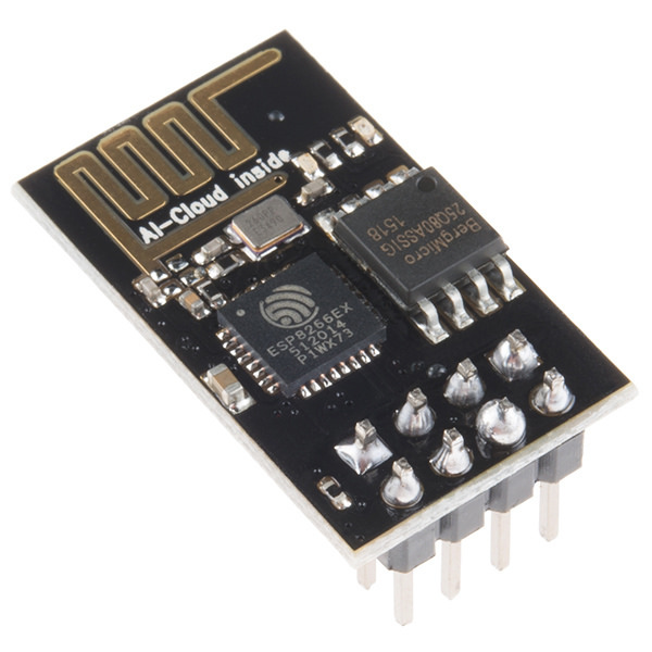
Figure 3.0 — ESP-01 module. File:ESP-01.jpg by Sparkfun Electronics. License: CC BY 2.0. Via Wikimedia Commons.
The ESP-01S is the cheapest WiFi add-on. ESP8266 inside, factory-loaded with AT-command firmware, four-pin UART interface plus power and enable.
3.1 Schematic theory
┌────────────┐                       ┌─────────────────┐
│ Side-header│                       │     ESP-01S     │
│            │                       │                 │
│ 3V3 ───────┼────────┬──────────────│ VCC             │
│            │        │              │                 │
│            │        ┴ C1 (10 µF) — │ GND             │
│            │        ┬              │                 │
│ GND ───────┼────────┴──────────────│ GND             │
│            │                       │                 │
│ TX0 ───────┼─[ R1 22Ω ]────────────│ RXD             │
│            │                       │                 │
│ RX0 ───────┼─[ R2 22Ω ]────────────│ TXD             │
│            │                       │                 │
│ 3V3 ───────┼─[ R3 10kΩ ]───────────│ EN              │
│            │                       │                 │
│ GP15 ──────┼─[ R4 1kΩ ]───────────-│ RST  (optional) │
└────────────┘                       └─────────────────┘
Notes:
- C1: 10 µF X7R or X5R bypass, placed within 5 mm of the ESP-01S VCC pin. The ESP-01S’s WiFi peaks pull 250 mA in 1 ms bursts; without local bulk capacitance the rail drops noticeably.
- R1, R2: 22 Ω series on TX/RX. Optional but recommended — dampens edge-rate ringing on the 115200-or-faster UART.
- R3: 10 kΩ pull-up on EN. ESP-01S has an internal pull-up but it’s not strong enough to be reliable in noisy environments.
- R4: 1 kΩ on RST line if you want software-driven reset; tie EN low briefly to reset. Optional — most users just power-cycle the whole device.
3.2 BOM
| Designator | Part | Source | Qty | Price ea |
|---|---|---|---|---|
| U1 | ESP-01S module | AliExpress / LCSC | 1 | $2-3 |
| C1 | 10 µF / 16 V X7R, 0805 | LCSC C18536 | 1 | $0.02 |
| R1, R2 | 22 Ω / 1% / 0603 | LCSC C23278 | 2 | $0.01 |
| R3 | 10 kΩ / 1% / 0603 | LCSC C25804 | 1 | $0.01 |
| R4 | 1 kΩ / 1% / 0603 | LCSC C21190 | 1 | $0.01 |
| J1 | 2.54 mm 2×9 pin female header | Mouser / LCSC | 1 | $0.30 |
Total BOM cost: ~$3 + PCB.
3.3 Layout
A 25 × 15 mm 2-layer board fits inside the case. Place the ESP-01S at one end, the female header opposite. The ESP-01S’s antenna is on the module; route the trace from your female-header’s edge to the module’s pin so the antenna ends up against the case’s edge (closer to the top of the kit, away from the speakers). The CYW43439 / ESP8266 antenna patterns are 50 Ω inverted-F — don’t put copper pours under the antenna section of the module.
A 3D-printed back from B05ESP.stl (Volume 3 §3.5) has clearance for this board; the antenna ends up in a small cutout for max range.
3.4 Premade alternatives
- Tindie ESP-01S adapters for the PicoCalc: ~$10 shipped. Search “PicoCalc ESP-01S” on Tindie. Not all in stock; checks out as community-quality, not vendor-grade.
- Generic ESP-01S breakout + jumpers: $5 total. Doesn’t fit cleanly inside the case but works on the bench.
3.5 Software side
- PicoMite: built-in
WEBcommands talk to the ESP-01S over UART0 at 115200. SetOPTION SERIAL CONSOLE COM2to free up COM1 for the ESP. PicoMite’sWEB CONNECT/WEB GET/WEB POSTsend AT commands transparently. - MicroPython: hand-roll AT or use one of the wrapper libraries (
micropython-esp01son PyPI; or one of the forum-published libraries). - Pico SDK C/C++:
pico_atlibrary or hand-roll. The ESP-01S’s AT spec is small (about 30 commands).
4. WiFi Add-on — ESP32 over SPI
Figure 4.0 — ESP32 development board. File:ESP32 Dev Board.jpg by Edwiyanto. License: CC BY-SA 4.0. Via Wikimedia Commons.
For higher throughput, an ESP32-class module wired SPI gives you 5-10× the bandwidth.
4.1 Schematic theory
┌────────────┐                            ┌────────────────┐
│ Side-header│                            │   ESP32-WROOM  │
│            │                            │                │
│ VBUS ──────┼─[ Q1 ]──[ U1 LDO 3.3 ]─────│ VDD3P3         │
│            │                            │                │
│ GND ───────┼────────────────────────────│ GND            │
│            │                            │                │
│ SCK (GP2) ─┼─[ R1 22Ω ]─────────────────│ SCK            │
│            │                            │                │
│ MOSI(GP3) ─┼─[ R2 22Ω ]─────────────────│ MOSI           │
│            │                            │                │
│ MISO(GP4) ─┼─[ R3 22Ω ]─────────────────│ MISO           │
│            │                            │                │
│ GP12 ──────┼─[ R4 1kΩ ]─────────────────│ CS_/EN         │
│            │                            │                │
│ GP13 ──────┼────────────────────────────│ HANDSHAKE      │
│            │                            │                │
│ GP14 ──────┼────────────────────────────│ /RESET         │
└────────────┘                            └────────────────┘

Q1 is a P-channel MOSFET acting as a load-switch — gates the ESP32's
power on/off via a Pico GPIO. The ESP32's >250 mA peaks would otherwise
disturb the side-header 3V3 budget.

U1 is a TPS62133 (or equivalent) buck LDO converting VBUS to 3.3 V at
1 A. Without USB-C plugged in, no 3.3 V → ESP32 doesn't boot. This is
acceptable for bench use; for battery-only operation, replace U1 with a
boost-buck from 3V3 (TPS63020 or similar).
The HANDSHAKE line is unusual but important: SPI master/slave with no flow control loses bytes when the slave can’t keep up. The ESP32 firmware (whether esp-at SPI variant or custom) raises HANDSHAKE when it has data ready or is buffer-full. The Pico waits on HANDSHAKE before sending.
4.2 BOM
| Designator | Part | Source | Qty | Price ea |
|---|---|---|---|---|
| U1 | TPS62133 1 A buck | Mouser | 1 | $1.50 |
| U2 (alt) | ESP32-WROOM-32E module (or DevKitC) | Espressif/LCSC | 1 | $5-10 |
| Q1 | AO3401 P-FET | LCSC C15127 | 1 | $0.05 |
| L1 | 4.7 µH inductor (for U1) | Coilcraft / LCSC | 1 | $0.30 |
| C1, C2 | 10 µF / 16 V X7R, 0805 | LCSC C18536 | 2 | $0.02 |
| C3, C4 | 22 µF / 6.3 V X7R, 0805 | LCSC C45783 | 2 | $0.04 |
| R1-R3 | 22 Ω / 1% / 0603 | LCSC C23278 | 3 | $0.01 |
| R4 | 1 kΩ / 1% / 0603 | LCSC C21190 | 1 | $0.01 |
| R5 | 100 kΩ / 1% / 0603 (Q1 gate pull-up) | LCSC C25741 | 1 | $0.01 |
| J1 | 2.54 mm 2×9 female header | Mouser / LCSC | 1 | $0.30 |
Total: ~$10 + PCB.
4.3 Layout
A 35 × 25 mm 4-layer board. Layer stackup: top-signal / GND / 3V3-power / bottom-signal. Keep the SPI traces (SCK, MOSI, MISO) length-matched to within 5 mm — at 25 MHz this barely matters but it’s good practice. The HANDSHAKE line has no timing requirement.
Place the ESP32 module so its antenna is over a cutout in the ground plane (typically a 12×6 mm clearance). The 4-layer ground pour helps thermals on the LDO; place a thermal via array under the LDO’s exposed pad.
4.4 Software side
esp-atSPI variant: https://github.com/espressif/esp-at. Espressif’s official AT firmware with a SPI transport. Build with the SPI factory config.micropython-esp32-spi-bridge: community Python library wrapping the SPI protocol. Cleaner than AT for high-throughput use.- Custom
esp32-spifirmware: if you want a specific protocol (SLIP-IP-over-SPI for full TCP/IP), Espressif’sesp-hostedframework is the toolkit.
4.5 Premade alternatives
- Adafruit ESP32 Feather V2: $20. Has its own onboard antenna or external U.FL. Not a drop-in for the side-header — you wire it to a breakout board you make yourself.
- AirLift FeatherWing: $13. Adafruit’s “WiFi co-processor” co-processor — slim ESP32 + a fixed pin map. Closer to drop-in.
- ClockworkPi forum custom boards: a few users have shared ESP32 carrier designs on the forum. Search “PicoCalc ESP32 carrier.”
5. I²S Audio DAC — PCM5102A
The clean fix for the PicoCalc’s mono-PWM audio (Volume 6 §15.3 covers the audio limitations).
5.1 Schematic theory
┌────────────┐                          ┌──────────────────┐
│ Side-header│                          │     PCM5102A     │
│            │                          │                  │
│ 3V3 ───────┼──────────────────────────│ VIN, AVDD, DVDD  │
│            │                          │                  │
│ GND ───────┼──────────────────────────│ AGND, DGND       │
│            │                          │                  │
│ I2S_BCLK ──┼─[ R1 22Ω ]───────────────│ BCK              │
│ (GP21)     │                          │                  │
│            │                          │                  │
│ I2S_LRCK ──┼─[ R2 22Ω ]───────────────│ LRCK             │
│ (GP22)     │                          │                  │
│            │                          │                  │
│ I2S_DIN ───┼─[ R3 22Ω ]───────────────│ DIN              │
│ (GP20)     │                          │                  │
│            │                          │                  │
│ 3V3 ───────┼──────────────────────────│ XSMT             │
│            │                          │                  │
│            │                          │ FMT ─── GND      │
│            │                          │ FLT ─── GND      │
│            │                          │ DEMP ── GND      │
│            │                          │                  │
│            │                          │ OUTL ─→ headphone L
│            │                          │ OUTR ─→ headphone R
│            │                          │ AGND ─→ headphone GND
└────────────┘                          └──────────────────┘
The PCM5102A has built-in 32 Ω headphone-driver — outputs go directly to a 3.5 mm TRS jack with no additional amp. AGND on the chip and on the headphone jack must be connected but should not overlap with the digital ground pour — common single-ground star topology with a 0 Ω resistor between digital and analog grounds works.
For driving the existing on-board speakers instead of headphones, route OUTL/OUTR through a small class-D amp (PAM8403, MAX98306) with appropriate gain.
5.2 BOM
| Designator | Part | Source | Qty | Price ea |
|---|---|---|---|---|
| U1 | PCM5102APWR | TI / Mouser | 1 | $3-5 |
| C1 | 10 µF / 16 V tantalum | LCSC C7176 | 1 | $0.10 |
| C2-C5 | 100 nF / 16 V X7R / 0603 | LCSC C14663 | 4 | $0.01 |
| C6, C7 | 2.2 µF / 6.3 V X7R / 0603 | LCSC C24611 | 2 | $0.02 |
| R1-R3 | 22 Ω / 1% / 0603 | LCSC C23278 | 3 | $0.01 |
| R4, R5 | 470 Ω / 1% / 0603 (output coupling) | LCSC C25085 | 2 | $0.01 |
| C8, C9 | 10 µF / 6.3 V tantalum (output couple) | LCSC C7176 | 2 | $0.10 |
| J1 | 3.5 mm TRS jack | Mouser CUI SJ-3523-SMT | 1 | $0.50 |
| J2 | 2.54 mm 2×9 female header | Mouser / LCSC | 1 | $0.30 |
Total: ~$5 + PCB.
5.3 Layout
The PCM5102A is sensitive to ground bounce — keep digital and analog ground planes separated and joined at a single star point under the chip’s exposed pad. Place output coupling caps within 5 mm of the headphone jack. Bypass caps within 3 mm of each VDD pin.
A 30 × 20 mm 4-layer board fits inside the kit’s case if you cut a 3.5 mm hole for the headphone jack on a custom 3D-printed back.
5.4 Premade alternatives
- Generic PCM5102A breakout from AliExpress: $3, but you wire it externally. Fits inside the case if you remove the speaker grille and place it sideways.
- Adafruit I²S 3 W Stereo Amp 1788: $6, includes a class-D amp. Drives speakers directly. Not as compact as the bare DAC.
5.5 Software side
The PCM5102A appears as a generic I²S DAC. Software paths:
- Pico SDK:
pico-extras/audio/audio_i2s.h. Configure for 16-bit / 44.1 kHz stereo. - MicroPython:
machine.I2S(0, sck=Pin(21), ws=Pin(22), sd=Pin(20), mode=I2S.TX, bits=16, format=I2S.STEREO, rate=44100, ibuf=4096). - PicoMite:
OPTION SOUND I2S 21,22,20then standardPLAY/PLAY MOD/PLAY WAVcommands.
6. LoRa Add-on — RFM95W (HopeRF)
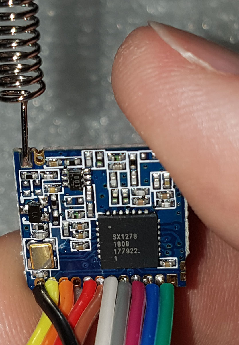
Figure 6.0 — LoRa transceiver module. File:LoRa Module with antenna and SPI wires attached.jpg by Cnd. License: CC0. Via Wikimedia Commons.
For sub-GHz long-range communications. 100 mW transmit, FSK or LoRa modulation.
6.1 Schematic theory
┌────────────┐                       ┌──────────────────┐
│ Side-header│                       │     RFM95W       │
│            │                       │   (915/868/433)  │
│ 3V3 ───────┼─[ C1 10µF ]──────────-│ VIN              │
│            │                       │                  │
│ GND ───────┼───────────────────────│ GND              │
│            │                       │                  │
│ SCK (GP2) ─┼─[ R1 22Ω ]────────────│ SCK              │
│ MOSI(GP3) ─┼─[ R2 22Ω ]────────────│ MOSI             │
│ MISO(GP4) ─┼─[ R3 22Ω ]────────────│ MISO             │
│            │                       │                  │
│ GP15 ──────┼─[ R4 1kΩ ]────────────│ NSS              │
│            │                       │                  │
│ GP14 ──────┼───────────────────────│ DIO0 (interrupt) │
│ GP13 ──────┼───────────────────────│ DIO1 (optional)  │
│ GP12 ──────┼───────────────────────│ RST              │
│            │                       │                  │
│            │                       │ ANT ─→ U.FL or 78 mm wire
└────────────┘                       └──────────────────┘
Antenna: at 915 MHz, a quarter-wave whip is 78 mm. Solder a 78 mm length of stiff wire (24 AWG copper) to the ANT pad and route it out a hole in the case. For higher gain, an external 915 MHz dipole with U.FL pigtail through an SMA connector (~$15 total).
6.2 BOM
| Designator | Part | Source | Qty | Price ea |
|---|---|---|---|---|
| U1 | RFM95W-915 (or -868 / -433) | LCSC / Mouser | 1 | $7-9 |
| C1 | 10 µF / 16 V X7R / 0805 | LCSC C18536 | 1 | $0.02 |
| C2 | 100 nF / 16 V X7R / 0603 | LCSC C14663 | 1 | $0.01 |
| R1-R3 | 22 Ω / 1% / 0603 | LCSC C23278 | 3 | $0.01 |
| R4 | 1 kΩ / 1% / 0603 | LCSC C21190 | 1 | $0.01 |
| J1 | U.FL connector (optional) | LCSC C2882721 | 1 | $0.30 |
| J2 | 2.54 mm 2×9 female header | Mouser / LCSC | 1 | $0.30 |
| Antenna | 78 mm wire OR U.FL dipole | bench / Adafruit | 1 | $0-15 |
Total: ~$8-15.
6.3 Layout
The RFM95W has a controlled-impedance RF input — keep the trace from the module’s ANT pin to the U.FL or wire-stub clean. 50 Ω microstrip if you can; otherwise just keep the trace short (<10 mm) and surrounded by ground.
6.4 Premade alternatives
- Adafruit RFM95W FeatherWing: $20. Includes a U.FL connector and a wire-stub trace. Wires to a separate breakout for PicoCalc use.
- HopeRF RFM95W bare module: $7 from LCSC, $9 from various AliExpress sellers. Use this for a custom board.
6.5 Software side
- MicroPython:
micropython-loralib(search GitHub for the most-current fork). Simpleradio.send(b"hello")/radio.recv(). - Pico SDK:
RadioLib(Arduino, also works in C). Much richer API. - PicoMite: a community CSUB exists for basic SX127x access.
7. Sub-GHz Hacking — CC1101
Cheaper alternative to the RFM95W, FSK/OOK only (no LoRa modulation), but the right radio for sub-GHz protocol research.
7.1 Schematic theory
Identical wiring topology to RFM95W (SPI + interrupt + chip-select), with one difference: CC1101 has separate GDO0 and GDO2 outputs that you can configure as different interrupt sources. Wire both to free Pico GPIO if you want full-flexibility code.
7.2 BOM
| Designator | Part | Source | Qty | Price ea |
|---|---|---|---|---|
| U1 | CC1101 module (E07-M1101D-TH) | LCSC / AliExpress | 1 | $3 |
| C1 | 10 µF / 16 V X7R | LCSC C18536 | 1 | $0.02 |
| R1-R4 | 22 Ω / 1% / 0603 | LCSC C23278 | 4 | $0.01 |
| R5 | 1 kΩ / 1% / 0603 | LCSC C21190 | 1 | $0.01 |
| J1 | 2.54 mm 2×9 header | Mouser / LCSC | 1 | $0.30 |
Total: ~$4.
7.3 Software side
- Picoware: Picoware (Volume 5 §5.10) has a CC1101 driver built-in. Useful for turnkey sub-GHz scanning.
- Pico SDK:
cc1101-picolibrary. Bare-metal control with full register access. - MicroPython: search GitHub for
micropython-cc1101.
8. Multi-Function Accessory Board — the “Dev Shield”
A useful design exercise: a single accessory board that combines several common needs. This is what I’d build for myself if I were to fab a single PCB.
8.1 Concept
A 50 × 35 mm 4-layer PCB on the side header, with:
- PCM5102A I²S DAC + 3.5 mm TRS jack (Section 5).
- CC1101 sub-GHz with U.FL connector for external antenna (Section 7).
- PN532 NFC over I²C — the missing RFID/NFC capability the kit lacks.
- BME280 environmental sensor (temp / humidity / pressure) over I²C — used as a “calibration” for any project that wants accurate ambient conditions. Pictured below.
- DS3231 RTC — battery-backed real-time clock so the device knows what time it is even after a full power cycle.
- Two qwiic / Stemma QT connectors — the standard 4-pin JST-SH for further I²C expansion.
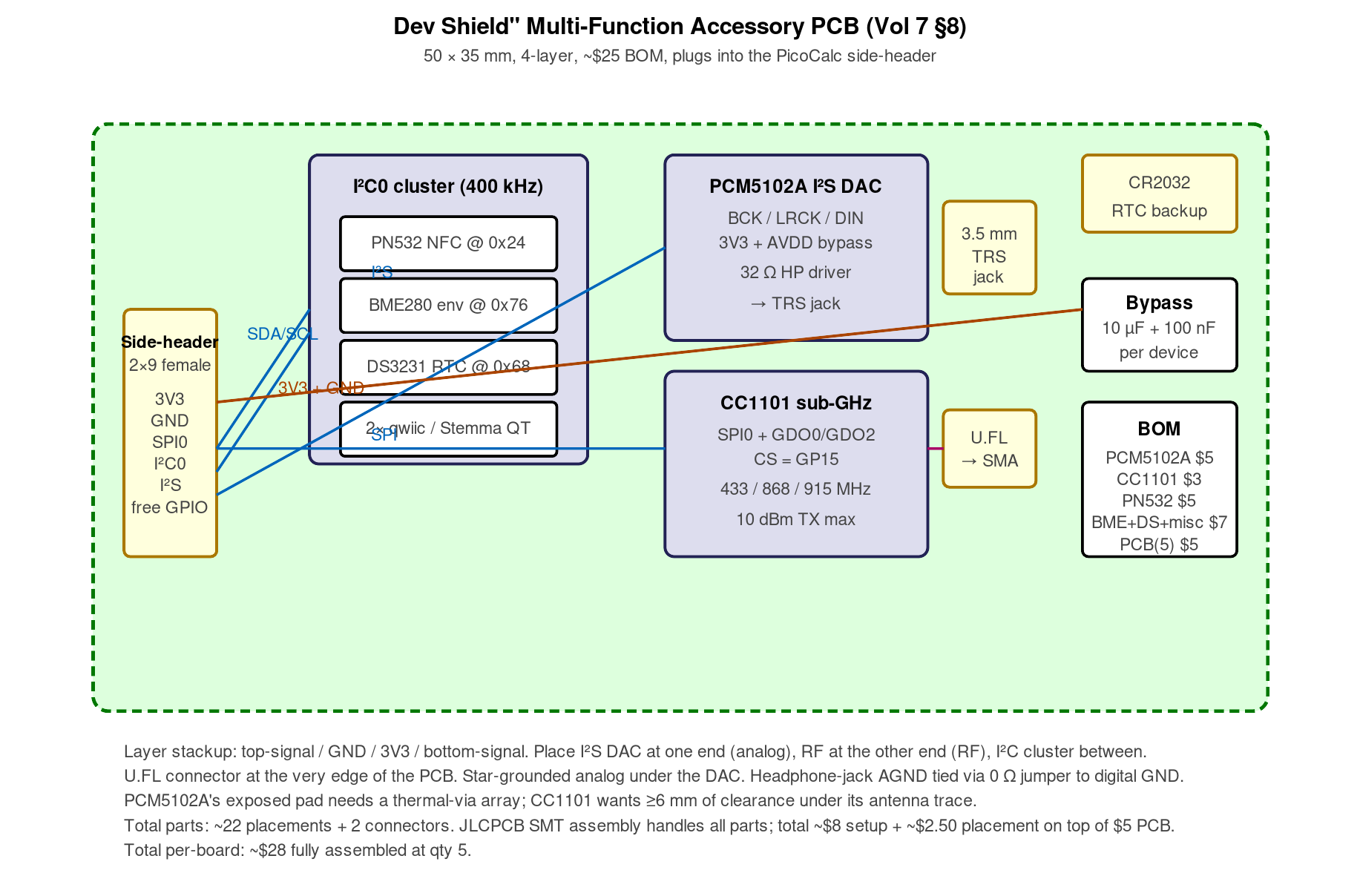
Figure 8.1 — Dev shield block diagram. Hand-authored for this volume.
8.2 Schematic theory — high level
The four I²C devices share I²C0 (GP4 SDA, GP5 SCL) at 400 kHz. PN532 at 0x24, BME280 at 0x76, DS3231 at 0x68, qwiic addresses are user-supplied. The SPI bus on GP2/3/4 is shared between the CC1101 and the PCM5102A’s I²S — wait, that’s a conflict. Re-do: I²S uses GP20/21/22 (a separate set), so SPI on GP2/3/4 is only used by the CC1101. Good.
Chip selects: CC1101 on GP15. (PCM5102A doesn’t have CS — it’s I²S only.)
Power: each device has its own bypass cap (10 µF + 100 nF). DS3231 needs a CR2032 backup battery for the RTC to survive main power loss; provide a small holder.
8.3 BOM
| Subsystem | Parts cost (approximate) |
|---|---|
| PCM5102A | $5 |
| CC1101 | $3 |
| PN532 | $5 (module) |
| BME280 | $4 (module) |
| DS3231 | $1 (chip + crystal + holder + battery) |
| Qwiic conn. | $0.50 × 2 |
| Discretes | ~$2 |
| Header | $0.50 |
| 3.5 mm jack | $0.50 |
| U.FL | $0.30 |
| PCB (5 pcs) | $5 |
| Total | ~$25-28 per board |
Figure 8.3 — BME280 breakout. File:BME280.jpg by Laserlicht. License: CC BY-SA 4.0. Via Wikimedia Commons.
8.4 Layout strategy
4-layer stackup: top-signal / GND / 3V3 / bottom-signal. Place the I²S DAC at one end (analog), the RF module at the other end (RF), and the I²C cluster in the middle. Keep the I²S DAC’s ground separate from the digital ground and join at a single point. Put the U.FL connector at the very edge of the PCB so the antenna trace is short.
8.5 Verdict
This is a “build once, useful forever” accessory. Total cost ~$25-30. Worth doing if you want the PicoCalc to be a multi-purpose lab instrument; less worth doing if you’re focused on a single use case.
9. The ZeroCalc Adapter — Pi Zero 2 W on the Pico Footprint
The most-popular “compute path D” adapter (Volume 8 covers the software side). Schematic theory below; if you want to roll your own instead of buying one, this is the recipe.
9.1 Theory of operation
The Pi Zero 2 W has a 40-pin GPIO header (2×20 at 2.54 mm). The PicoCalc carrier has a 40-pin Pico-shaped socket (2×20 at 2.54 mm). The adapter is a small PCB that:
- Presents a Pico-pinout 40-pin male header on the bottom (drops into the socket).
- Has a 40-pin female header on the top (Pi Zero 2 W mounts to it).
- Wires the Pi Zero’s pins to the Pico-equivalent functional pins on the bottom side, so the kit’s LCD/SD/keyboard/audio all light up.
The pin remapping is the work. A Pico has GP0-GP28 with multiple peripheral functions per pin (PWM, SPI, I²C, UART, ADC, PIO). A Pi Zero has GPIO0-GPIO27 with similar function multiplexing. The adapter board must route the function not the pin number — so the carrier’s “SPI0 SCK on Pico GP10” must end up on the Pi Zero’s GPIO11 (which is the Pi’s SPI0 SCK).
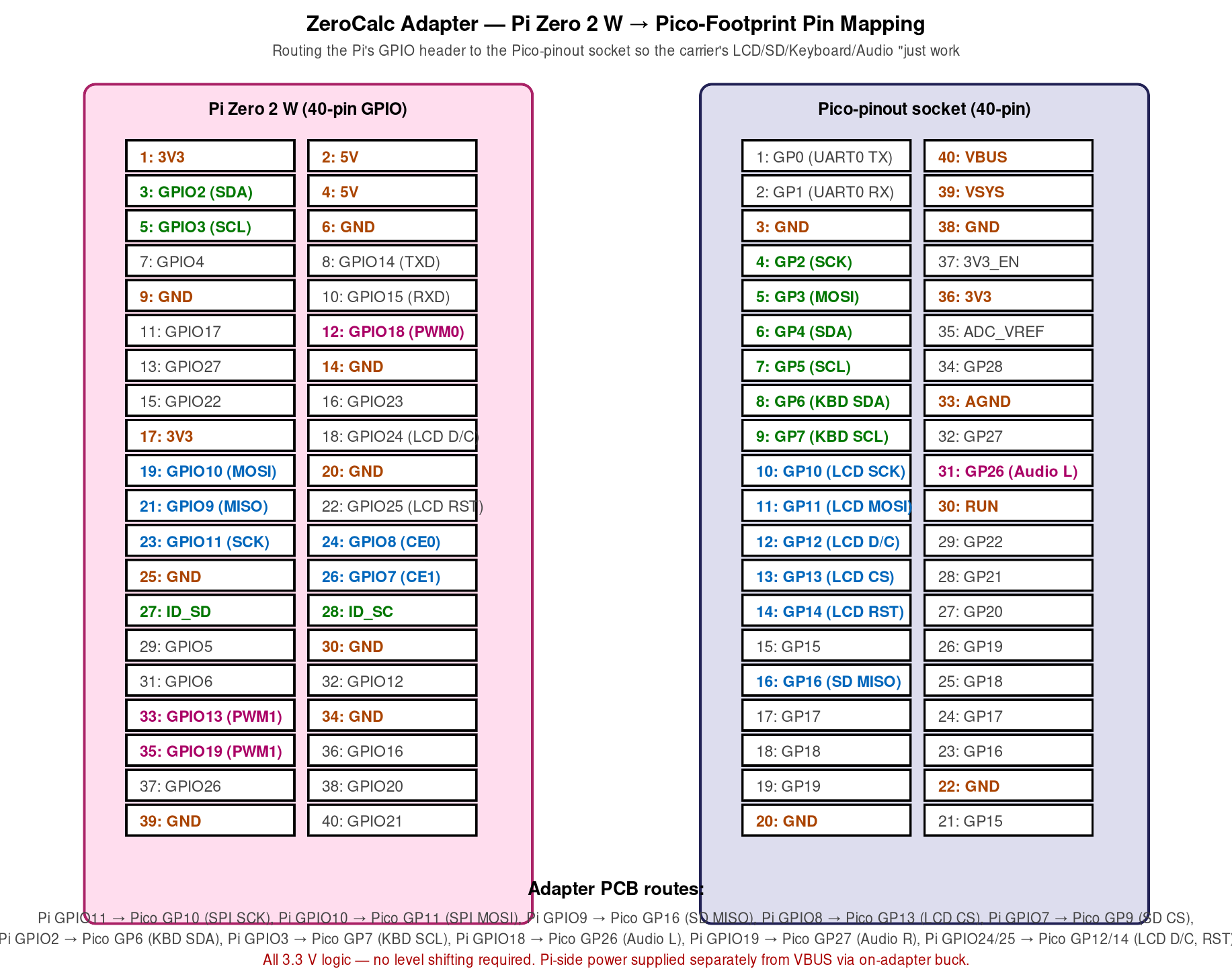
Figure 9.1 — ZeroCalc adapter pin mapping. Hand-authored for this volume.
9.2 Pin-mapping table (verified against ClockworkPi v2.0 r3)
| Carrier function | Pico pin | Pi Zero pin (GPIO) | Notes |
|---|---|---|---|
| LCD SCK | GP10 | GPIO11 (SPI0 SCK) | direct |
| LCD MOSI | GP11 | GPIO10 (SPI0 MOSI) | direct |
| LCD D/C | GP12 | GPIO25 | GPIO; software-driven |
| LCD CS | GP13 | GPIO8 (SPI0 CE0) | direct |
| LCD RESET | GP14 | GPIO24 | GPIO |
| SD SCK | GP10 | shared with LCD SCK | same SPI bus |
| SD MISO | GP12 | GPIO9 (SPI0 MISO) | direct |
| SD CS | GP9 | GPIO7 (SPI0 CE1) | direct |
| KBD I2C SDA | GP6 | GPIO2 (I2C1 SDA) | direct |
| KBD I2C SCL | GP7 | GPIO3 (I2C1 SCL) | direct |
| Audio L | GP26 | GPIO18 (PWM0) | direct |
| Audio R | GP27 | GPIO19 (PWM1) | direct |
| USB | (Pico) | (Pi Zero microUSB) | physically routed |
The adapter’s bottom side also exposes the Pico’s other GPIOs (the ones the Pi Zero doesn’t use) on test points — useful for bringup debugging.
9.3 Logic-level concerns
The Pi Zero 2 W is a 3.3 V GPIO platform. So is the PicoCalc carrier. No level shifting required. The adapter is a pure copper-trace mapper.
9.4 Power
The Pi Zero 2 W draws ~120 mA idle, ~250 mA active, ~500 mA peak under load. This is significantly over the 3V3 budget the carrier was designed for. The adapter must supply Pi Zero power separately:
- Option A: dedicated buck from VBUS to 5V/3A. Powers the Pi Zero; the carrier’s 3V3 budget is no longer a concern. Adapter has its own LDO. Requires USB-C plugged in.
- Option B: dedicated buck from BATT_P (the cell pack). Powers the Pi Zero from battery. Requires opening up battery routing in the kit.
- Option C: pass-through Pi Zero’s own micro-USB to a dedicated wall-wart. Easiest but ugly.
Most premade ZeroCalc adapters go with Option A (USB-C-powered), which is fine for daily-driver use because Pi Zero battery life is limited anyway (~3 hours). Option B is the elegant solution if you want any meaningful battery operation; it requires careful BOM (a 5 V boost from BATT_P that handles the 3.0-4.2 V cell-voltage range).
9.5 Mechanical fit
A Pi Zero 2 W is 65 × 30 mm. The PicoCalc’s case has ~70 × 35 mm of clearance above the carrier socket. The Pi Zero fits, but barely — it sticks slightly above the carrier and the case’s standard rear shell won’t close. You need a 3D-printed back (Volume 3 §3.5; the B05XXXX.stl blank is a starting point, but most builders use a custom modification).
9.6 Premade ZeroCalc adapters
- Original ZeroCalc (community-designed, sold on Tindie via various sellers): $18-22.
- PicoCalc Trixie adapter by user
cuuon the forum: revised version with a permanent USB-C cutout at the rear; $25-30 from Tindie. - GitHub project
ZeroCalc-PCB(open source, you fab): KiCad files at https://github.com/topics/zerocalc. Search for the most-current fork.
9.7 DIY recipe — fabbing your own
- Open the GitHub KiCad project (or design from scratch — about 1-2 evenings of work for someone with KiCad experience).
- Verify the pin-mapping table against your carrier-board revision.
- Generate gerbers — JLCPCB’s standard 4-layer 1.6 mm 1 oz copper ENIG is fine.
- Order the PCB and stencil — JLCPCB does both for ~$15 total qty 5 (with stencil ~$10 extra).
- Source parts: 40-pin male header, 40-pin female header, buck IC (LMR16006 or TPS62133), inductor, caps. ~$3-4 BOM.
- Assemble — for 4-layer the headers are through-hole; the buck IC is QFN, reflow-only.
- Test — verify 5 V output before plugging the Pi Zero in.
- Plug in the Pi Zero, drop the assembly into the carrier socket, boot.
10. The Lyra Adapter
The Luckfox Lyra (Volume 9) is a smaller SoC than the Pi Zero, so its adapter is smaller and simpler. Lyra-Plus is the Plus variant of the Lyra family, with on-module 128 MB LPDDR3 RAM and a microSD slot. The adapter routes the Lyra’s MIPI-DSI display interface to the carrier’s LCD’s SPI port through a converter chip — that’s the interesting part.
10.1 The display-interface conversion
The Lyra’s RK3506 SoC outputs MIPI-DSI for the display, but the carrier’s LCD is SPI. Two solutions:
- Software: bit-bang the LCD over the Lyra’s SPI peripheral, just like the Pico does. Slow, but works. The Buildroot configurations Volume 9 §9.5 covers all use this path.
- Hardware: convert MIPI-DSI to a compatible LCD bus via a bridge IC (TC358762 or SSD2828). This gets you 60 fps full-screen at the cost of a more complex adapter.
Most Lyra-Plus adapters use the software path. Performance is limited but adequate for terminal use, slow for video.
10.2 The pin map
| Carrier function | Pico pin | Lyra pin | Notes |
|---|---|---|---|
| LCD SCK | GP10 | SCLK0 | direct |
| LCD MOSI | GP11 | TXD0 | direct |
| LCD D/C | GP12 | GPIO0_C0 | direct |
| LCD CS | GP13 | GPIO0_C1 | direct |
| LCD RESET | GP14 | GPIO0_C2 | direct |
| SD SCK | shared | shared SPI | shared with LCD |
| SD MISO | GP12 | RXD0 | direct |
| SD CS | GP9 | GPIO0_C3 | direct |
| KBD I2C SDA | GP6 | I2C2_SDA_M0 | direct |
| KBD I2C SCL | GP7 | I2C2_SCL_M0 | direct |
| Audio L | GP26 | I2S0_SDO | use external I²S DAC, not PWM |
| Audio R | GP27 | I2S0_SDO | (single I²S, stereo via timing) |
Note that the Lyra’s SoC architecture wants I²S audio out, not PWM. So the Lyra adapter typically includes a small PCM5102A on the same PCB — saves the user from also building a separate audio shield.
10.3 Power
Lyra-Plus draws ~80 mA idle, ~200 mA active, ~400 mA peak. Significantly less than Pi Zero. Adapter can power it from VBUS via a smaller LDO; battery operation is feasible from a buck-LDO on BATT_P.
10.4 Premade Lyra adapters
- Luckfox-spec adapter: ~$15-20 from Luckfox direct or AliExpress. Multiple form-factor variants.
- Community ClockworkPi forum adapter (search “Lyra adapter”): hand-assembled, ~$25 with shipping.
- 3D-printable backs in
05-resources/3D Print Files/(Volume 3 §3.5):B05LYP.stl,B05LYR.stl,B05LYU.stl,B04LYC.stlfor various Lyra variants.
11. Programmer / Debugger Adapter — Pico Probe Permanent Mount
The Raspberry Pi Debug Probe is a Pico-shaped device that exposes SWD and UART. Most users plug it into the carrier’s SWD test points with jumpers; for permanent dev work, embedding it inside the case is much nicer.
11.1 Mechanical
The Pico Probe is 51 × 21 × 8 mm. It fits inside the kit if you use a 3D-printed back with a USB-A passthrough cutout on the rear (Odd Inventor’s “PicoCalc back with Pico Probe port” on Printables is the reference design — Volume 3 §3.5).
11.2 Wiring (bench)
Three jumpers from the probe’s debug port to the carrier’s SWD test points (SWDIO, SWCLK, GND). For permanent install: solder a 4-pin header to the carrier’s SWD test points, plug the probe’s debug cable in, route the probe’s USB-A out the rear passthrough.
11.3 Software
OpenOCD on the host, with interface/cmsis-dap.cfg and target/rp2040.cfg (or rp2350.cfg). VS Code’s “Raspberry Pi Pico” extension auto-detects the probe.
The probe also exposes a separate UART port that can pick up the Pico’s UART output for serial-console debugging. Convenient when USB CDC is busy (BOOTSEL mode, mass-storage active).
12. PCB Fabrication and Assembly Workflow
Pulling all of this together, the actual workflow for a hobbyist EE producing one of these accessory boards:
12.1 Design
- Schematic capture in KiCad. Symbol library: KiCad standard library covers most parts; custom symbols for ESP-01S, RFM95W, CC1101 are easy to make from datasheets.
- PCB layout. 2-layer for simple boards (under 30 mm of routing), 4-layer for anything with controlled-impedance traces or significant power distribution.
- Design rules — JLCPCB’s standard 4-layer is 6 mil/6 mil/8 mil hole/spacing/track. Comfortable for everything in this volume.
12.2 Fabrication
- JLCPCB: cheapest, fastest (3-day production + 5-day shipping). 4-layer 5×5 cm at qty 5 = $5.
- PCBWay: similar pricing, slightly different finish options.
- OSH Park: more expensive ($10-15 for 5×5 cm at qty 3), gold ENIG by default, made in the US.
12.3 Assembly
- Hand-soldering: works for everything 0603 and larger plus SOIC/TSSOP/SOT-23. QFN/QFP requires either a stencil + reflow or hot-air rework. Generally fine for accessory boards.
- JLCPCB SMT: $8 setup fee + ~$0.10 per placed part. Worth it for QFN/QFP-heavy boards. They have a parts catalog covering most generics; non-stocked parts get a markup.
- Hot-plate reflow + stencil: $50 hot plate + $10 stencil from the PCB house = a useful in-house assembly station for small runs.
12.4 Validation
- Power-on test: 3V3 rail at the right voltage before plugging in the carrier. AVOID: don’t plug an unverified accessory into the carrier’s 3V3 — a short can damage the AXP2101.
- I²C/SPI scan: write a small Pico-side test program that probes the bus and verifies expected responses.
- Functional test: stack-specific test program exercising each peripheral on the accessory.
13. Side-Header Mechanical Concerns
A few mechanical details that catch first-time accessory designers:
13.1 Header height
The kit’s case has a side cutout sized for headers ≤6 mm above the carrier PCB. Standard 2.54 mm female headers with 8.5 mm plastic shrouds are too tall — they hit the case. Use low-profile 2.54 mm female headers (5.0 mm shroud, available from Mouser as “tall” or “short” variants).
13.2 PCB thickness
For a side-header accessory that lives outside the case, 1.6 mm PCB is fine. For an accessory that needs to fit inside the case (between the carrier and the rear shell), 1.0 mm PCB is necessary — extra clearance for the cell pack underneath.
13.3 Connector orientation
The kit’s side cutout is on the right edge of the case. Accessories should orient their female header on the left edge of the accessory PCB so that, when the accessory plugs in, it sticks out to the right of the case. Reversing this puts the accessory inside the case mechanically.
14. Resources
14.1 EDA tools
| Tool | Link | Notes |
|---|---|---|
| KiCad 8+ | https://www.kicad.org/ | Free, open source |
| Altium Designer | https://www.altium.com/ | Commercial, expensive |
| Eagle (Autodesk) | https://www.autodesk.com/eagle | Older, free version limited |
| EasyEDA | https://easyeda.com/ | Web-based, integrates with LCSC parts |
| Flux.ai | https://www.flux.ai/ | AI-assisted EDA, modern web tool |
14.2 PCB fab houses
| House | Link | Strengths |
|---|---|---|
| JLCPCB | https://jlcpcb.com | Cheapest, fastest, SMT assembly |
| PCBWay | https://www.pcbway.com | Similar to JLC; slightly different finishes |
| OSH Park | https://oshpark.com | US-made, gold ENIG default |
| Eurocircuits | https://www.eurocircuits.com | Europe, low quantities |
| Aisler | https://aisler.net | Europe, hobbyist-friendly |
14.3 Component suppliers
| Supplier | Link | Strengths |
|---|---|---|
| LCSC | https://www.lcsc.com | Cheapest for generic discretes, JLC SMT compatible |
| Mouser | https://www.mouser.com | Best for STM32, named-brand parts |
| Digi-Key | https://www.digikey.com | Same league as Mouser |
| Adafruit | https://www.adafruit.com | Polished modules, breakouts |
| SparkFun | https://www.sparkfun.com | Same; complementary inventory |
| Pimoroni | https://shop.pimoroni.com | Pico-Plus 2 boards, polished modules |
| Espressif Direct | https://www.espressif.com | Reference dev boards, SoCs |
| Coilcraft | https://www.coilcraft.com | Best inductors |
14.4 ClockworkPi-specific
| Resource | Link |
|---|---|
| ClockworkPi GitHub | https://github.com/clockworkpi/PicoCalc |
| Schematic | https://github.com/clockworkpi/PicoCalc/blob/master/clockwork_Mainboard_V2.0_Schematic.pdf |
| 3D-printable backs (community) | https://www.printables.com/model/1253552-picocalc-back-with-pico-probe-port |
| Modular back design (Kelpiscool) | https://github.com/Kelpiscool/picocalc-modular-back |
| ZeroCalc adapter projects | https://github.com/topics/zerocalc |
| Forum DIY thread (PicoCalc accessories) | https://forum.clockworkpi.com/c/picocalc/ |
14.5 Component datasheets
Footnotes
-
JLCPCB — https://jlcpcb.com. Default 5×5 cm 4-layer at $2 for qty 5 in 2026; actual cost depends on copper weight, thickness, surface finish. ↩