Flipper Zero · Volume 10
Flipper Zero Volume 10 — DIY Modules
GPIO header reference, KiCad templates, mechanical envelope, sample DIY projects, PCB-from-scratch checklist
10.1 About this Volume
When the right module doesn’t exist commercially — or when you want a specific feature combination at a lower BOM cost than buying — DIY is the answer. A bench with full PCB fab + small-scale assembly makes this tractable cost-wise; the hard part is getting the GPIO mapping, mechanical envelope, and Flipper-side firmware integration right. This volume covers all three.
10.2 The Header — KiCad / EDA-side reference
10.2.1 The connector spec
The Flipper’s GPIO header is a 2×9 (18-pin) 1.27 mm pitch female header on the device side. The matching male connector on a daughter PCB is 2×9 1.27 mm pitch. Most modules use a press-fit header for tool- free attach/detach.
Vendors and part numbers:
Table 1 — Vendors and part numbers
| Part | Function | Vendor / LCSC |
|---|---|---|
| Standard 2×9 1.27 mm header (male) | Daughter PCB → Flipper | Multiple; LCSC C155829 (generic) |
| 2×9 1.27 mm SMD header (low profile) | Same, lower stack height | LCSC C496497 |
| 2×9 1.27 mm right-angle | Daughter PCB exits horizontally | LCSC C492447 |
The press-fit fitting on the Flipper side wears with insertion cycles — not a serious concern under 100 mate cycles, becoming noticeable past ~500. Treat it as semi-permanent.
10.2.2 KiCad and Eagle libraries
Two open libraries cover the connector + Flipper outline:
kbembedded/flipper-gpio-eda— KiCad and Eagle symbol/footprint libraries for the Flipper GPIO connector. Use this rather than re-drawing the part. Pairs cleanly with KiCad 7+.lomalkin/flipperzero-protoboards-kicad— KiCad protoboards designed against the published GPIO pinout. The canonical starter for any DIY GPIO board. Open license, uses the community’s reverse-engineered footprint.
Drop either library into your *.lib/*.kicad_sym includes; the
connector symbol exposes net names matching the docs.flipper.net pinout
table (Vol 7 §2).
10.2.3 The mechanical envelope
The “mechanical envelope” is the volume above the Flipper’s top edge where a module can extend without hitting the Flipper’s body or buttons. Approximate dimensions (verify against your specific device):
Width:    ~76 mm (Flipper body width, no fenders)
Depth:    ~20-25 mm (module depth above the GPIO header — varies)
Height:   ~30-40 mm of usable Z above the header before mechanical
          interference with Flipper button cluster

Above ~40 mm Z is fine - just ensure the module doesn't overhang
back-side away from the Flipper body more than ~5 mm without support
(prevents snap-off in pocket).
The community mechanical envelope spec is documented at flipper.wiki
hardware-overview and in the 3D models repo
(flipperdevices/flipperzero-3d-models). 3D-print the Flipper body STL
and lay your daughter PCB on top to verify fit before fabricating.
10.2.4 Cases — printable
- MuddledBox/FlipperZeroCases — Apache-licensed STLs for hard covers including “GPIO covered” and “GPIO open” variants.
- fivesixzero “Case for Flipper Zero Wi-Fi Module v1” — Printables.com #179910, the cleanest open-license case for the ESP32-S2 devboard footprint. Useful as a baseline shell to extend.
- TruTech / fivesixzero forks on Printables for module-specific shells (Mayhem, Game Over, etc.).
10.3 Pin-Budget and Routing Discipline
10.3.1 Three rules that prevent most DIY pain
- Don’t draw more than ~150 mA continuous from the 3V3 rail. Multi-radio designs need their own boost converter or USB-C input.
- Tie unused GPIO pins to ground or pull them high through 10–100 kΩ pull-up resistors. Floating MCU inputs draw irregular current and pick up noise. The Flipper firmware doesn’t drive every pin every cycle; treat the header as if pins might be high-Z.
- Use the 1-Wire pin (17) for low-frequency single-bit signals only. It’s electrically connected to the iButton pad and to the firmware’s 1-Wire master — collision is at best annoying, at worst destructive.
10.3.2 Power
If your module needs > 50 mA, take it from the 5 V GPIO pin (1) with a buck regulator down to your needed voltage, rather than from 3V3. The 5 V rail off USB has plenty of headroom; the boost from battery is weaker but still better than the 3V3 sub-rail.
If your module must run on the 3V3 rail directly (small sensors, discrete radios), use a soft-start cap (10 µF + 0.1 µF on the input) to absorb inrush.
10.3.3 Signal levels
All Flipper I/O is 3.3 V tolerant only. Level-shift externally if your slave runs at 5 V. Common shifters:
- 74LVC1T45 — single-channel bi-directional, auto-direction. Tiny.
- TXB0104 / TXB0108 — 4 / 8 channel, auto-direction.
- MOSFET pair (BSS138 + 10 kΩ + 10 kΩ) — discrete, slow but cheap.
For UART → 5 V TTL, the 74LVC1T45 chain is what most ESP32 daughterboards use. For I²C → 5 V, the BSS138 chain is the reference. Don’t try to direct-connect a 5 V part to the Flipper — even a 50-pin signal swing above 3.6 V can stress the MCU clamp diodes over time.
10.4 Sample DIY Projects
10.4.1 DIY ESP32-C6 / S3 Daughterboard
The official WiFi Devboard is stuck on ESP32-S2 (no BLE 5, no Thread/ Matter, no 802.15.4). DIY route:
- KiCad: drop a Seeed XIAO ESP32-C6 (or ESP32-S3) onto a
lomalkinprotoboard. - Wire UART: ESP32 RX → Flipper pin 13 (TX, PB6). ESP32 TX → Flipper pin 14 (RX, PB7). GND, 3V3.
- Add a USB-C connector for direct flashing + standalone power.
- Drop a BOOT/RESET button pair for ESP32 flashing in case the Flipper-side flasher fails.
- Flash FlipperHTTP (jblanked’s repo supports C5/C6/S3) or Marauder-fork-with-BLE5 for BLE 5 attacks.
Total BOM: $5–8 ESP32 dev module + $0.50 USB-C + $0.20 buttons + $1 header + $2 PCB. Under $15 turnkey.
The Apex 5 (Vol 9 §2.4) is the closest commercial answer with ESP32-C5; the DIY route is cheaper and customizable.
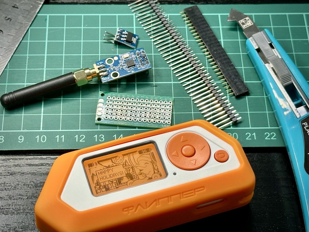
10.4.2 DIY NRF24 board on a perfboard
NRF24L01+ on bare 5-pin SPI is ~$3 from Aliexpress. Drop one on a perfboard, wire to GPIO pins per Vol 8 §4.3, slap it in a 3D-printed shell. 30 minutes start to finish.
For longer range, get the “NRF24L01+ Long Range PA+LNA” variant with SMA antenna (~$8). 100 m+ MouseJack range.
10.4.3 DIY IR-blaster boost stage
A higher-power IR transmitter for 30+ ft range:
        +5V GPIO (pin 1)
            │
            ├─── 220 µF cap (buffer)
            │
   ┌────────┤
   │        │
   ▼        │
  IR LED    │  3 in series
  IR LED    │  (940 nm, e.g. Everlight IR333C)
  IR LED    │
   │        │
   ├────────┘
   │
   ▼  10 Ω 1 W  (current limit; calc: (5V - 3*1.5V) / 10 = 50 mA peak)
   │
   ▼
  BC337 / 2N3904 NPN
   │   collector
   │
   ── BASE: 1 kΩ → Flipper PA7 (pin 2, output via TIM PWM, carrier 38 kHz)
   │
   ▼
  GND
Wire to Flipper pin 2 (PA7) via the 1 kΩ base resistor. Configure Unleashed/Xtreme/RogueMaster IR app → External GPIO → Send=A7. Done. Range jumps from 5 m to ~30+ ft.
Refine with a high-gain LED (Vishay TSAL6100, 80 mW/sr) and the range goes another 2–3×.
10.4.4 DIY GPS module
Buy a $5 NEO-6M from Aliexpress. Wire:
NEO-6M VCC → Flipper 3V3 (pin 9)
NEO-6M GND → Flipper GND (pin 8 or 11 or 18)
NEO-6M TX  → Flipper RX (pin 14, PB7)
NEO-6M RX  → Flipper TX (pin 13, PB6) [optional; for AT commands]
3D print a small case that clips above the GPIO header. Install
ezod/flipperzero-gps FAP. ~$5 turnkey GPS.
10.4.5 DIY Environmental Sensor Pack
I²C is on pins 15 (SDA, PC1) and 16 (SCL, PC0). Drop:
- BME280 — temperature, humidity, pressure (~$3, 0x76 or 0x77)
- BMP680 — gas + IAQ (~$8, 0x76 or 0x77)
- MH-Z19B — CO2 (~$25, UART or PWM)
- VEML7700 — ambient light (~$3, 0x10)
All on the same I²C bus (different addresses). FAPs:
quen0n/unitemp-flipperzerofor BMP/BME/HTU/DHT/DS18B20kamylwnb/bme680_flipper_zerofor BME680- DIY MicroFAP for MH-Z19 (UART) — straight read of CO2 every 5 sec
Total kit BOM under $40 for a four-sensor pack.
10.4.6 DIY OBD-II carrier (ELM327 + level shift)
Wire an ELM327 module’s UART to Flipper UART through a 5 V → 3.3 V level shifter. Connect the OBD-II side to vehicle. Custom FAP queries ELM327 ATZ/ATSP6/0100, decodes responses. Useful for read-only vehicle diagnostics from the Flipper UI.
Variant: bare CAN transceiver (MCP2515 + MCP2562) on SPI. Read raw CAN frames. Substantially more useful for protocol RE work.
10.4.7 DIY Audio I²S DAC
The Flipper has no audio DAC, but DIY one:
- PCM5102 I²S DAC module (~$5)
- Bit-bang I²S on three GPIO pins: BCK (bit clock), LRCK (left/right clock), DATA. Use timer-driven IRQ to clock samples at 44.1 kHz.
Performance: limited by how fast the firmware can shovel samples. Quality depends on FAP — typical I²S-bit-bang on STM32WB55 reaches 22 kHz / 8-bit PCM comfortably; 44.1 / 16-bit needs DMA + timer help that’s harder to get right from a FAP. Easier path: use a UART-driven I²S DAC like the Maxim MAX98357 — accepts a serial bitstream rather than I²S clocks.
10.4.8 Pin-extender / breakout headers
The simplest DIY: a 2×9 1.27 mm header on top, a 2×9 1.27 mm header on bottom, all 18 pins straight through. Lets you use the Flipper GPIO with jumper wires while a “real” module also stacks on top. Sometimes called a “pin-passthrough adapter”.
10.5 Reference Open-Hardware Projects
These are existing open designs to study, not necessarily build:
zst123/FCFZ— “Fully Compatible Flipper Zero” on Hackster.io. Open hardware that mimics the Flipper pinout. Useful for understanding what GPIO behaviors the Flipper firmware actually expects from a module.GthiN89/FuckingCheapFlipperZero— Hackaday.io #203021. Off-the- shelf-module DIY Flipper alternative running Momentum, ~€10–30 BOM. Good schematic/firmware reference.UberGuidoZ/Flipper— the GPIO/ folder is the largest community pinout/wiring reference: ESP32, ESP8266, ESP32-CAM, NRF24, plus DSTIKE Deauther wiring. The de-facto map.- Hackaday’s flipper-zero tag — a steady drip of one-off DIY boards: AS7331 UV (full custom I²C library), CAN-bus shields, low-power FM transmitters, hall-effect probes, LoRaWAN nodes. Use as starter templates.
- Lab401 LightMessenger — POV-stick LED column on the GPIO header. Open design. A worked example of “trivial GPIO + clever FAP = real product”.
10.6 The PCB-from-Scratch Checklist
Each step has a deliverable.
10.6.1 Spec phase
- Block diagram: every IC, every connector, every power rail.
- Power budget: peak + continuous current per rail. Numbers, not “should be fine”.
- GPIO assignment table: which Flipper pin does what. Reserve unused pins as “FUTURE” with explicit pull state.
- Mechanical sketch: bounding box, connector placements, height
envelope. Verify against
flipperzero-3d-models.
10.6.2 Schematic phase
- Schematic in KiCad using the
kbembedded/flipper-gpio-edasymbol library. Power flags on every rail. - Decoupling: 0.1 µF + 1 µF on every IC’s VDD pin.
- Level shifters wherever a 5 V signal meets the Flipper.
- Test points on every signal you might want to scope post-fab. At least: each rail, UART RX/TX, SPI MOSI/MISO/SCK, any clock.
- ESD protection on user-facing connectors (USB, antenna SMA).
10.6.3 Layout phase
- 2-layer for simple cards, 4-layer for radio/multi-radio.
- Ground plane on bottom (2L) or layer 2 + 3 (4L).
- Crystal placement: as close to the IC as possible, with stitch vias around the trace pair.
- Antenna routing: 50 Ω controlled-impedance microstrip (for 4-layer 0.8 mm with FR4, that’s ~0.36 mm wide). Keep ≥ 5 mm from any noisy switching node.
- 3D check — load the STEP into FreeCAD, verify the connector doesn’t fight the Flipper edge.
- DRC clean before sending to fab. Don’t assume the fab catches it; it doesn’t.
10.6.4 Fab + assembly
- JLCPCB / PCBWay spec: 4-layer, 0.8 mm, ENIG, edge bevel if you want a clean USB-C insert.
- Stencil if reflowing — 0.1 mm thick laser-cut.
- Reflow profile matched to your paste (typically Sn63Pb37 lead if you’re doing rework, SAC305 if you’re going production-style).
- First-article test: power up at 0.5 A current limit on bench supply. If the supply hits limit, it’s a short — power off immediately, troubleshoot. Don’t assume.
10.6.5 Bring-up
- Power rails verified with multimeter on each test point.
- MCU enumerated via SWD before exercising the Flipper.
- Each subsystem tested independently before integration. Don’t debug 3 things at once.
- Flipper-side FAP written to exercise each signal. Don’t expect the production FAP to “just work” — the simple test FAP isolates hardware bugs from firmware bugs.
10.7 Common DIY-Specific Pitfalls
Table 2 — 7. Common DIY-Specific Pitfalls
| Pitfall | Symptom | Fix |
|---|---|---|
| Running 5 V signal into Flipper GPIO | MCU clamp diodes degrade; Flipper resets eventually | Always level-shift |
| Drawing > 150 mA from 3V3 | Flipper resets during module activity | External power for high-current modules |
| Forgetting to GND-bond unused GPIO | Floating pins pick up noise; readings flap | Pull down (or up) every unused pin |
| Wrong-polarity connector | Module doesn’t power up; possibly damages IC | Match the 18-pin pinout exactly; verify with a probe before powering |
| Inserting NRF24/CC1101 daughterboard backwards (in modules with a sub-slot) | Magic smoke from one or both | Key the slot in your design; never trust orientation |
| Multi-radio TX during HDMI streaming on VGM-stack | Wi-Fi/Sub-GHz TX power 6-10 dB lower | Schedule TX to not overlap HDMI active |
| Forgetting the 1.27 mm pitch | Fabbed PCB doesn’t mate with Flipper | KiCad library has the right pitch — use it |
| Not testing in pre-production | Catch a layout bug at production scale | Always order a 2-board prototype first |
10.8 The 3V3 Rail Watchdog Pattern
For DIY designs that absolutely must run on the 3V3 rail (no external USB), add a watchdog:
3V3 IN ──┬──── To module
         │
         ▼
        100 mΩ shunt resistor
         │
         ▼
  ADC pin (e.g. PC0 / pin 16) on the Flipper, sampled
  by your FAP at 100 Hz. If voltage across the shunt
  exceeds 15 mV (= 150 mA), throttle module activity.
Software cheap, hardware cheap, prevents brown-outs on edge-case TX profiles. None of the commercial multi-radio modules do this — you can.
10.9 PCB Tools That Are Worth Knowing
For a lab with full equipment:
- KiCad 7+ for schematic + layout. Free, open. The community standard.
- DipTrace or Eagle if you’ve already got muscle memory.
- FreeCAD for STEP-level mechanical verification. Import the
Flipper’s STEP from
flipperzero-3d-models. - JLCPCB / PCBWay for fab. JLCPCB cheaper, 4-layer 0.8 mm at $20 for 5 boards; turnaround 7–10 days incl. shipping.
- Stencil from JLCPCB as part of the same order; good quality.
- For assembly: hand-paste with a manual stencil + reflow oven works well at 5–10 board volumes. JLCPCB SMT service is worth it past 20 boards.
10.10 What’s next
Vol 11 — Workflows & Recipes. End-to-end field workflows: garage-door analysis, RFID badge audit, BLE keyboard pentest, NFC tag programming, ham/SDR companion-mode with HackRF/RTL-SDR, qFlipper + Mobile App workflows.
Comments (0)