HaleHound · Volume 3
HaleHound Volume 3 — The Radios
CC1101, NRF24L01+PA+LNA, PN532 V3 and GPS on one shared VSPI bus — schematic-grade pinouts, per-board CS differences, and the independent-buck rule
3.1 About this Volume
This volume is the electrical reference for the four external radios HaleHound-CYD drives, plus the ESP32’s own built-in Wi-Fi/BLE radio for completeness. It is the schematic-grade companion to the two build walkthroughs: the Classic build (Vol 5, exposed-SPI CYD + Cinder Ferret carrier) and the Fire Weasel build (Vol 6, integrated board). Where those volumes say “wire the CC1101 per the pinout table,” this is that table — and the reasoning behind every pin.
Four modules sit outside the ESP32:
- CC1101 — sub-GHz transceiver, scoped by the firmware to 300–439 MHz.
- NRF24L01+PA+LNA — 2.4 GHz transceiver with power amplifier and low-noise amplifier.
- PN532 V3 (Elechouse) — 13.56 MHz NFC/RFID front end, run in SPI mode.
- GPS — GT-U7 or NEO-6M (the complete units and Fire Weasel kit ship the ATGM336H with a ceramic patch antenna), a plain 9600-baud NMEA receiver on a UART.
Three of those four (CC1101, NRF24, PN532) ride the same VSPI bus that the on-board microSD card already uses — GPIO 18/19/23. The GPS is the exception: it is a UART device and lands on the CYD’s serial header, which is also the ESP32’s USB console, and that collision is handled in firmware rather than in copper.
Every GPIO number, header name and CS assignment in this volume comes from the v4.0 firmware README’s wiring diagrams, which are authoritative and are reproduced (adapted to box-drawing form) below. The CYD breakout map — which GPIO is on which 1.25 mm connector — is cross-checked against the Sunton/witnessmenow reference for the ESP32-2432S028R and the LCDwiki documentation for the ESP32-32E “E32” boards. Nothing here is invented; where a board behaves differently from the base CYD, the difference is called out with the reason.
Note — Firmware licence and lineage. HaleHound-CYD is proprietary firmware (© 2026 Jesse C. Hale, all rights reserved; free to flash and run, source not published), forked from CiferTech’s MIT-licensed ESP32-DIV (2023). The electrical interface documented here is HaleHound’s own; one of its deliberate corrections to the inherited ESP32-DIV wiring is the CC1101 TX/RX swap discussed in §4. Do not describe the firmware as open source — unlike SquachWatch (GPL-3.0) or nyanBOX (MIT), the HaleHound source is closed.
3.2 The shared VSPI bus and SPI arbitration
The ESP32 exposes two general-purpose SPI peripherals to application code: HSPI and VSPI. On the Cheap Yellow Display the division of labour is fixed by the board, not by HaleHound:
- HSPI drives the TFT panel (ILI9341 or ST7796), on GPIO 12/13/14 with CS/DC/RST and the backlight on their own pins. The display is a write-mostly, high-bandwidth bus that HaleHound overclocks for redraw speed; it is never shared with a radio.
- VSPI is the ESP32’s “other” SPI, on GPIO 18 (SCK) / 19 (MISO) / 23 (MOSI). The on-board microSD card already sits on VSPI with its own chip-select. HaleHound hangs the CC1101, the NRF24 and the PN532 on the same three signal lines, each with its own CS.
That is the single most important electrical fact about the platform: the three external SPI radios and the SD card are all on one bus. SPI is a multi-drop bus by design — SCK, MOSI and MISO fan out to every device, and only the device whose chip-select is asserted LOW listens or talks. The constraint is that exactly one CS may be active at any instant; assert two and both devices drive MISO and the bus is garbage.
                 CYD ESP32 — VSPI bus (shared)
                 ┌───────────────────────────────┐
   GPIO 18 SCK  ─┤───┬──────┬──────┬──────┬───────┤
   GPIO 23 MOSI ─┤─┐ │    ┌─┘    ┌─┘    ┌─┘        │
   GPIO 19 MISO ─┤ │ │  ┌─┘    ┌─┘    ┌─┘          │
                 └─┼─┼──┼──────┼──────┼────────────┘
                   │ │  │      │      │
               ┌───▼─▼┐ │      │      │
               │microSD│ │      │      │   each device
               │ CS 5  │ │      │      │   has its OWN
               └───────┘ │      │      │   chip-select:
                     ┌───▼──┐ ┌─▼───┐ ┌▼─────┐
                     │CC1101│ │NRF24│ │PN532 │
                     │CS 27 │ │CSN 4│ │SS 17 │   (base CYD pins)
                     │ /21  │ │ /26 │ │      │
                     └──────┘ └─────┘ └──────┘
Figure 3.1 — VSPI is a multi-drop bus: SCK/MISO/MOSI fan out to the SD card and all three external SPI radios; only the asserted CS gets the bus. Pin numbers are the base ESP32-2432S028 (“esp32-cyd”) assignments; per-board variants are in §9.
HaleHound resolves the one-at-a-time constraint in software with an SPI manager that arbitrates the bus — it deselects whatever was active, reconfigures the bus for the next device’s clock polarity/phase and speed, asserts the new CS, does the transaction, and releases. The practical consequences for a builder:
- Wiring is trivial, timing is not. SCK/MOSI/MISO are literally three wires shared by everyone, so the harness is small. But the radios cannot run truly concurrently on the bus; the firmware time-slices them. The only genuinely simultaneous dual-radio operations are the ones that pair a VSPI radio with the ESP32’s internal Wi-Fi/BLE (which is not on VSPI at all) — e.g. the drone-detect mode that runs the NRF24 and the ESP32 Wi-Fi promiscuous sweep on separate cores.
- A misbehaving device poisons the bus for all. An NRF24 that browns out and holds MISO, or a PN532 left asserted, takes down SD logging and the other radios too. This is why the decoupling and power rules in §5 and §8 matter beyond just the module that breaks.
- CS pins are the scarce resource, not the data pins. The base CYD has very few free GPIO after the display, touch, SD and RGB LED are accounted for. HaleHound reclaims the three RGB-LED pins (GPIO 4/16/17) and the two spare header pins (GPIO 22/27) to find enough chip-selects and control lines. That reuse is why the LED does not function as a status light on a built HaleHound, and why the CS assignments shift between boards (§9).
Note — Why the SD card and radios coexist at all. Many CYD firmwares avoid external SPI radios precisely because VSPI is “taken” by the SD slot. HaleHound’s position is that the SD card is low-duty (loot writes,
.subreads, OTA) and the radios are bursty, so an arbitrated share is acceptable. Expect occasional contention under heavy simultaneous logging; it is a design tradeoff, not a fault.
3.3 The CYD breakout map the radios hang off
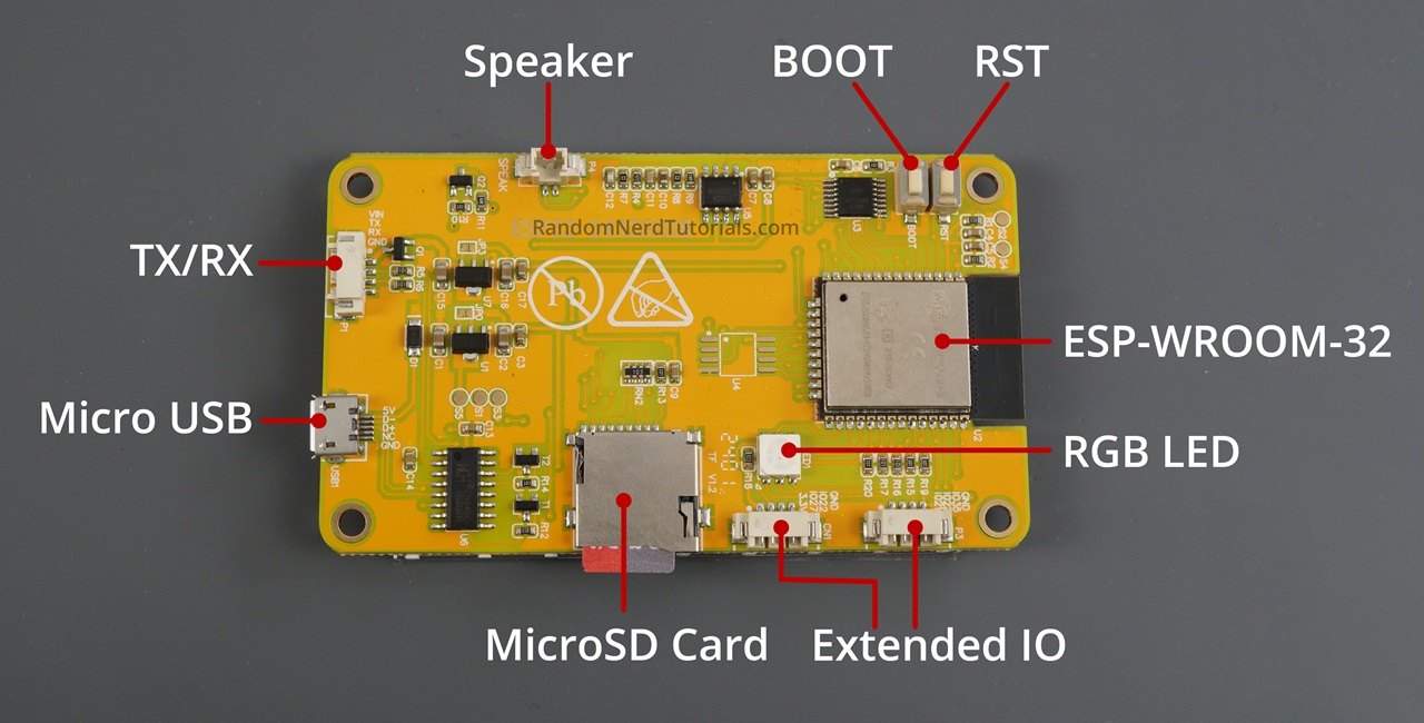
Every external module lands on one of the CYD’s four 1.25 mm expansion connectors, or on a pin reclaimed from the RGB LED. Knowing which GPIO is on which connector is half the build, so it is worth stating once. All expansion connectors are 4-pin 1.25 mm (Molex PicoBlade / “MX1.25” style) except the 2-pin speaker header:
  ┌──────────────── CYD expansion connectors (base ESP32-2432S028) ───────────────┐
  │  P1  (serial)   VIN  │ GPIO1  TX  │ GPIO3  RX  │ GND                           │
  │  P3  (GPIO)     GND  │ GPIO35 (input-only) │ GPIO22 │ GPIO21 (backlight on 2.8")│
  │  CN1 (I²C-ish)  GND  │ GPIO22 │ GPIO27 │ 3.3 V                                 │
  │  P4  (speaker)  2-pin, off GPIO26 through the on-board amplifier               │
  └────────────────────────────────────────────────────────────────────────────────┘
  Reclaimed from the RGB LED (base CYD: common-anode R/G/B):
     GPIO 4  (was LED red)    GPIO 16 (was LED green)    GPIO 17 (was LED blue)
Figure 3.2 — The CYD’s expansion headers and the three RGB-LED pins HaleHound repurposes. GPIO 35 is input-only (it has no output driver), which is exactly why it is used as a radio receive/status input rather than a control output.
Two facts from this map drive everything downstream:
- GPIO 21 vs GPIO 27 is the backlight-vs-CS swap. On the 2.8” ESP32-2432S028 the panel backlight is on GPIO 21, leaving GPIO 27 free on CN1 for a chip-select. On the 3.5” QDtech E32R35T the backlight moves to GPIO 27, so GPIO 27 is no longer free and the CC1101 CS has to move to GPIO 21. This single difference is the origin of the per-board CS table in §9 — it is not arbitrary, it follows the backlight pin.
- GPIO 1/3 are the USB-serial UART (UART0). The P1 “serial” connector breaks out the exact pins the CH340 USB bridge uses to talk to the ESP32. Putting the GPS there means the GPS and the USB console fight for the same UART — handled in firmware (§7), not by a jumper.
The base CYD has two independent 3.3 V LDO regulators — one for the ESP32, one for the TFT (witnessmenow documents the separate test points S2 and S5). Neither is sized to feed a 20 dBm power amplifier on top of its normal load; that is the entire reason the Ebyte PA modules need their own buck (§8).
Figure 3.3 — The CYD breakout hardware: the expansion headers (P1/P3/CN1) and the RGB-LED pins HaleHound reclaims are all on this board. Photo: generic CYD reference.
3.4 CC1101 — sub-GHz radio
The CC1101 is a Texas Instruments sub-1-GHz OOK/2-FSK/GFSK/MSK transceiver. HaleHound uses
it for capture, replay, brute-force code generation, spectrum display and .sub playback.
Two physical forms appear: the bare HW-863 module (stock, ~+12 dBm TX) and the
E07-433M20S (a CC1101 plus a 20 dBm power amplifier — the amplified option, wired
differently; see §8).
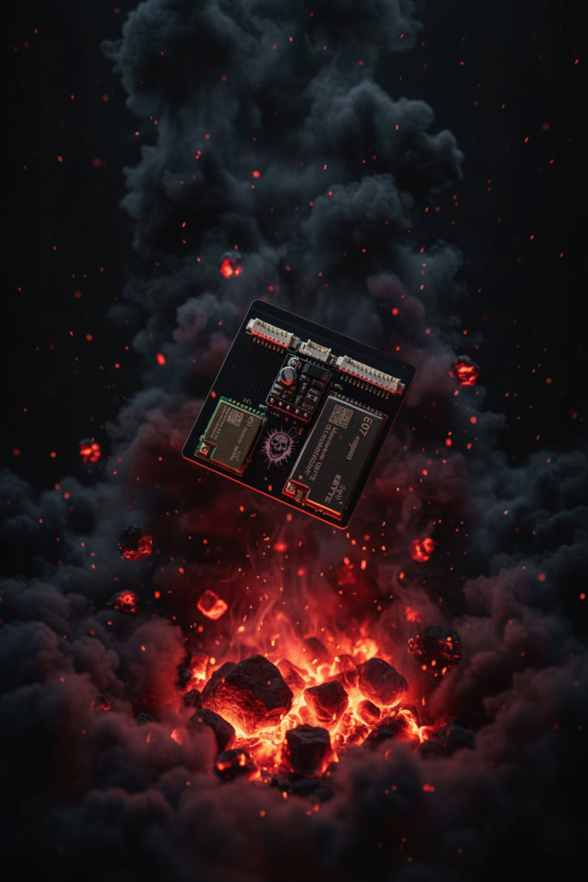
Figure 3.4 — The Cinder Ferret carrier (Classic build, Vol 5) mounts the sub-GHz, 2.4 GHz and NFC radios on one board that bridges to the CYD’s exposed VSPI pins. Photo: HaleHound.com.
3.4.1 Stock HW-863 pinout
┌─────────────────┐              ┌──────────────────────┐
│    CC1101       │              │     CYD ESP32        │
│    HW-863       │              │                      │
├─────────────────┤              ├──────────────────────┤
│ VCC ────────────┼──────────────┤ 3.3 V                │
│ GND ────────────┼──────────────┤ GND                  │
│ SCK ────────────┼──────────────┤ GPIO 18   (VSPI SCK) │
│ MOSI ───────────┼──────────────┤ GPIO 23   (VSPI MOSI)│
│ MISO ───────────┼──────────────┤ GPIO 19   (VSPI MISO)│
│ CS  ────────────┼──────────────┤ GPIO 27   (CN1 hdr)  │
│ GDO0 (TX) ──────┼──────────────┤ GPIO 22   (P3 hdr)   │
│ GDO2 (RX) ──────┼──────────────┤ GPIO 35   (P3 hdr)   │
└─────────────────┘              └──────────────────────┘
Figure 3.5 — CC1101 (HW-863) to base ESP32-2432S028. GDO0 is the transmit data line (ESP32 → radio); GDO2 is receive (radio → ESP32). Adapted from the v4.0 README.
Table 1 — 4.1 Stock HW-863 pinout
| CC1101 pin | ESP32 GPIO | Header | Function | Notes |
|---|---|---|---|---|
| VCC | 3.3 V | CN1 | Power | Stock HW-863 may share the CYD 3.3 V rail; the E07 PA must not (§8) |
| GND | GND | CN1 | Ground | Common ground is mandatory |
| SCK | 18 | — | VSPI clock | Shared with SD + NRF24 + PN532 |
| MOSI | 23 | — | VSPI data in | Shared |
| MISO | 19 | — | VSPI data out | Shared |
| CS | 27 (2.8”) / 21 (3.5”) | CN1 / — | Chip-select | Moves with the backlight pin (§4.3) |
| GDO0 | 22 | P3 | TX data | ESP32 → radio |
| GDO2 | 35 | P3 | RX data | radio → ESP32; GPIO 35 is input-only, which suits an RX line |
3.4.2 The GDO0/GDO2 TX/RX correction
HaleHound inherits its CC1101 driver lineage from CiferTech’s ESP32-DIV, and the README is explicit that the parent firmware had the CC1101 TX and RX pins swapped. HaleHound corrects this: GDO0 is TX (to the radio), GDO2 is RX (from the radio). This matters to a builder for two reasons. First, if you port a wiring harness or a pin map from an ESP32-DIV build or a third-party tutorial, check the GDO assignment against this table — a swapped pair will usually init the radio fine (the SPI config path is independent of GDO) but then fail to transmit or capture, which reads as a “dead radio” that passes self-test. Second, GPIO 35 being input-only is consistent with GDO2 = RX: the ESP32 physically cannot drive GPIO 35, so it can only ever be a receive/status input, which is what GDO2 is.
3.4.3 Per-board CS difference
The CC1101 chip-select is the pin that moves between boards, and it moves for one reason — the backlight:
Table 2 — the backlight
| Board | Backlight pin | CC1101 CS | Why |
|---|---|---|---|
ESP32-2432S028 2.8” (esp32-cyd) | GPIO 21 | GPIO 27 | GPIO 27 free on CN1 |
QDtech E32R28T 2.8” (esp32-e32r28t) | GPIO 21 | GPIO 27 | Same as base CYD |
QDtech E32R35T 3.5” (esp32-e32r35t) | GPIO 27 | GPIO 21 | Backlight took 27, so CS moves to 21 |
NM-RF-Hat 2.8” (esp32-cyd-hat) | GPIO 21 | GPIO 27 | Base-CYD layout |
All other CC1101 pins (SCK/MOSI/MISO/GDO0/GDO2) are identical across every board. Only CS moves. Pick the build target that matches your board and the firmware drives the correct CS automatically; the only time this bites a builder is when hand-wiring a carrier for a 3.5” unit and routing CS to the wrong pad.
3.4.4 TX power and frequency scope
Stock, the CC1101 transmits at setPA(12) — about +12 dBm. With the E07-433M20S PA
module and PA mode enabled (Settings → CC1101 Module → E07), output rises to +20 dBm.
The firmware scopes CC1101 operation to 300–439 MHz — this is the band the modes are
tuned and curated for, even though the vendor store page advertises the chip’s full
“300–928 MHz” silicon range. Treat 300–439 MHz as the operating envelope; 433.92 MHz and
315 MHz are the two anchor frequencies most modes default to.
3.5 NRF24L01+PA+LNA — 2.4 GHz radio
The NRF24 is a Nordic 2.4 GHz GFSK transceiver; the “+PA+LNA” variant adds a front-end
power amplifier and low-noise amplifier on an SMA-pigtail board. HaleHound drives it at
RF24_PA_MAX (about +20 dBm with the PA) for 2.4 GHz scanning, promiscuous sniffing,
MouseJack-class injection, BLE-advertising-channel work and broadband carrier output.
3.5.1 Pinout
┌─────────────────┐              ┌──────────────────────┐
│  NRF24L01       │              │     CYD ESP32        │
│  +PA+LNA        │              │                      │
├─────────────────┤              ├──────────────────────┤
│ VCC ────────────┼──────────────┤ 3.3 V (see power §8) │
│ GND ────────────┼──────────────┤ GND                  │
│ SCK ────────────┼──────────────┤ GPIO 18   (VSPI SCK) │
│ MOSI ───────────┼──────────────┤ GPIO 23   (VSPI MOSI)│
│ MISO ───────────┼──────────────┤ GPIO 19   (VSPI MISO)│
│ CSN ────────────┼──────────────┤ GPIO 4    (was LED R)│
│ CE  ────────────┼──────────────┤ GPIO 16   (was LED G)│
│ IRQ (optional) ─┼──────────────┤ GPIO 17   (was LED B)│
└─────────────────┘              └──────────────────────┘
Figure 3.6 — NRF24L01+PA+LNA to base ESP32-2432S028. CSN/CE/IRQ reuse the three common-anode RGB-LED pins. Adapted from the v4.0 README.
Table 3 — 5.1 Pinout
| NRF24 pin | ESP32 GPIO | Function | Notes |
|---|---|---|---|
| VCC | 3.3 V (or buck) | Power | E01-2G4M27SX PA variant must use the independent buck (§8) |
| GND | GND | Ground | Common ground |
| SCK | 18 | VSPI clock | Shared |
| MOSI | 23 | VSPI data in | Shared |
| MISO | 19 | VSPI data out | Shared |
| CSN | 4 (base) / 26 (E32 boards) | SPI chip-select | Reclaimed LED-red pin on base CYD |
| CE | 16 | Chip-enable (TX/RX mode) | Reclaimed LED-green pin |
| IRQ | 17 | Interrupt (optional) | Reclaimed LED-blue pin; can be left open |
3.5.2 Per-board CSN difference
Table 4 — 5.2 Per-board CSN difference
| Board | NRF24 CSN | Why |
|---|---|---|
ESP32-2432S028 2.8” (esp32-cyd) | GPIO 4 | LED-red pin reclaimed |
| QDtech E32R28T / E32R35T | GPIO 26 | GPIO 4 is used for the CC1101 PA TX_EN on these boards (§8) |
| NM-RF-Hat 2.8” | GPIO 4 | Base-CYD layout |
CE (16) and IRQ (17) are the same on every board. Only CSN moves, and it moves on the E32 boards specifically because GPIO 4 is needed as the E07 PA’s TX enable there.
3.5.3 The 10 µF decoupling capacitor
The single most common NRF24+PA+LNA failure is random resets — the module reboots or drops off the bus mid-operation. The cause is the PA’s switching current: when the amplifier keys up it pulls a current spike the thin module trace and the shared rail cannot supply without the local supply voltage dipping below the NRF24’s brown-out threshold. The fix is a 10 µF capacitor soldered directly across the module’s VCC and GND pins, as close to the chip as possible, to act as a local charge reservoir for the PA key-up transient.
        NRF24L01+PA+LNA module
        ┌───────────────────────┐
   VCC ─┤●───────┬──────────────┤
        │        │10µF          │   solder the cap AT the module,
        │       ═╪═ (electro-    │   not at the ESP32 end — the
   GND ─┤●───────┴  lytic/MLCC)  │   trace inductance is what bites
        └───────────────────────┘
Figure 3.7 — The 10 µF reservoir cap across the NRF24 module’s own VCC/GND pads.
Tip — Cap first, then blame the rail. On a stock (non-PA) NRF24 the cap alone often cures resets. On the E01-2G4M27SX PA module the cap is necessary but not sufficient — a 27 dBm-class PA needs its own buck supply (§8) as well as local decoupling. Fit both, then test.
3.5.4 Power note
A plain NRF24L01+PA+LNA breakout can usually run from the CYD 3.3 V rail with the 10 µF cap fitted. The Ebyte E01-2G4M27SX — the high-power NRF front end shipped in some kits — is in the same category as the E07 sub-GHz PA: it must be fed from the independent 3.3 V buck, not the CYD rail. See §8.
3.6 PN532 V3 — NFC/RFID
The PN532 is an NXP 13.56 MHz contactless front end. HaleHound uses the Elechouse PN532 V3 board specifically, run in SPI mode so it can join the VSPI bus with the other radios. The PN532 supports I²C, SPI and HSU (high-speed UART); the mode is chosen by the board’s two on-board DIP switches.
3.6.1 Pinout
┌─────────────────┐              ┌──────────────────────┐
│    PN532 V3     │              │     CYD ESP32        │
│   (Elechouse)   │              │                      │
├─────────────────┤              ├──────────────────────┤
│ VCC ────────────┼──────────────┤ 3.3 V   (CN1 hdr)    │
│ GND ────────────┼──────────────┤ GND     (CN1 hdr)    │
│ SCK ────────────┼──────────────┤ GPIO 18 (VSPI SCK)   │
│ MOSI ───────────┼──────────────┤ GPIO 23 (VSPI MOSI)  │
│ MISO ───────────┼──────────────┤ GPIO 19 (VSPI MISO)  │
│ SS  ────────────┼──────────────┤ GPIO 17 (was LED B)  │
└─────────────────┘              └──────────────────────┘
Figure 3.8 — PN532 V3 to base ESP32-2432S028, SPI mode. SS reuses GPIO 17. Adapted from the v4.0 README.
Table 5 — 6.1 Pinout
| PN532 pin | ESP32 GPIO | Function | Notes |
|---|---|---|---|
| VCC | 3.3 V | Power | From CN1; the PN532 is a modest load, CYD rail is fine |
| GND | GND | Ground | Common ground |
| SCK | 18 | VSPI clock | Shared |
| MOSI | 23 | VSPI data in | Shared |
| MISO | 19 | VSPI data out | Shared |
| SS | 17 | Chip-select | Shares the GPIO 17 pin with the NRF24 IRQ line |
3.6.2 DIP-switch setting for SPI mode
The Elechouse PN532 V3 selects its host interface with two DIP switches. For HaleHound’s SPI mode:
        PN532 V3 DIP block
        ┌──────────────┐
        │  ┌──┐  ┌──┐   │     CH1 = OFF
        │  │▼ │  │ ▲│   │     CH2 = ON
        │  └──┘  └──┘   │     → SPI mode
        │  CH1   CH2    │
        └──────────────┘
Figure 3.9 — PN532 V3 DIP switches set to SPI: CH1 OFF, CH2 ON.
Getting this wrong is the usual PN532 “not detected” fault: the board defaults to I²C or HSU out of the bag, and in those modes it never answers on the SPI bus no matter how correct the wiring is. Set CH1 OFF / CH2 ON, power-cycle, and the SS line on GPIO 17 will bring it up.
3.6.3 Bundling note and alternatives
The PN532 is listed as a required module in the firmware README but is no longer bundled with several current SKUs — the complete 4” and 3.5” units and the Fire Weasel kit ship without it (“neither is the PN-532 … installed”). It is an add-it-yourself part. The RFID menu also offers two alternative back ends the firmware can target instead of a wired PN532: a Chameleon Ultra connected over BLE (NTAG read/write and mfkey32 recovery), and an ST25R3916 that is present in the menu as a stub (the RFAL driver is still in development). For a wired on-board NFC front end the PN532 V3 in SPI mode is the only fully supported choice.
3.7 GPS — GT-U7 / NEO-6M and the UART0 conflict
The GPS is the one external module that is not on the SPI bus. It is a plain NMEA receiver that streams position sentences over a UART at 9600 baud (the GT-U7 default). HaleHound uses it for wardriving (GPS-tagged AP logging), the Flock You ALPR-camera geolocation saves, and a live satellite/NMEA view. Supported receivers: the GT-U7 and the NEO-6M; the complete units and Fire Weasel kit ship the ATGM336H with a ceramic patch antenna, which is a compatible 9600-baud NMEA module.
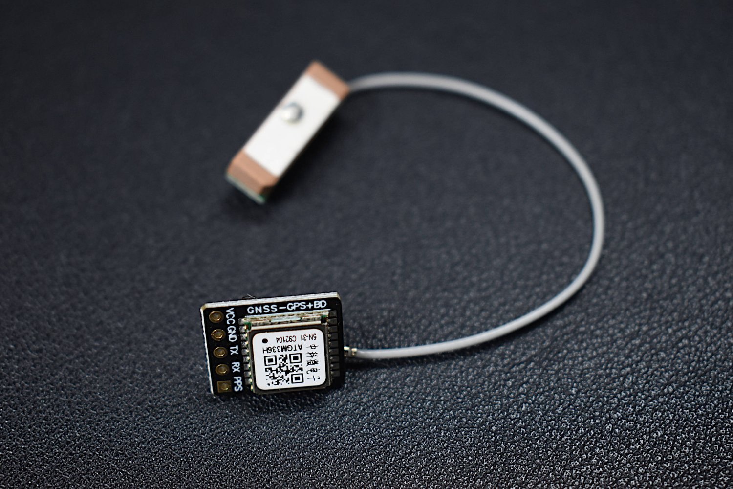
Figure 3.10 — The GPS receiver is a plain 9600-baud NMEA module on a UART, not an SPI device. Photo: representative GPS module (ATGM336H class).
3.7.1 Pinout
┌─────────────────┐              ┌──────────────────────┐
│    GT-U7        │              │  CYD P1 Connector    │
│    GPS          │              │  (serial JST header) │
├─────────────────┤              ├──────────────────────┤
│ VCC ────────────┼──────────────┤ VIN                  │
│ GND ────────────┼──────────────┤ GND                  │
│ TX  ────────────┼──────────────┤ TX = GPIO 1          │
│ RX (not used) ──┼──────────────┤ RX = GPIO 3          │
└─────────────────┘              └──────────────────────┘
Figure 3.11 — GPS onto the CYD’s P1 serial header. The GPS TX (module output) goes to the P1 “TX” pin = GPIO 1. The GPS is receive-only here; its RX is unused. Adapted from the v4.0 README.
Table 6 — 7.1 Pinout
| GPS pin | CYD pin | Function | Notes |
|---|---|---|---|
| VCC | VIN (P1) | Power | Takes board input voltage, not the regulated 3.3 V |
| GND | GND (P1) | Ground | Common ground |
| TX | GPIO 1 (P1 “TX”) | Module → ESP32 | Works on every board |
| RX | GPIO 3 (P1 “RX”) | Unused | Receive-only; leave open |
3.7.2 The UART0 conflict and how firmware handles it
GPIO 1 and GPIO 3 are the ESP32’s UART0 pins — the same lines the CH340 USB bridge uses for the serial console and for flashing. A device on P1 therefore shares the wire with the USB serial port. HaleHound handles the collision in firmware rather than asking the builder to add a jumper or switch:
- When a GPS mode starts, the firmware calls
Serial.end()to detach UART0 so the GPS owns the line. - When the GPS mode exits, UART0 is restored so the USB console works again.
- The firmware auto-scans GPIO 1 / 3 / 26 at GPS start, so it locks onto the receiver regardless of which pin a given board routes it to.
Board-specific behaviour: the GPS TX → GPIO 1 path works on every board. The 3.5” E32R35T and the factory-built sale units lock GPS only on GPIO 1; the 2.8” boards also tolerate GPIO 3. Because of the auto-scan this is usually invisible, but if a hand-wired GPS does not lock on a 3.5” unit, move its TX to the GPIO 1 pin.
Warning — Do not expect serial logs with the GPS live. Because UART0 is detached while a GPS mode runs, you will not get USB serial console output during wardriving. This is expected, not a fault. Exit the GPS mode to get the console back.
3.8 The independent 3.3 V buck for the Ebyte PA modules
This is the rule that most often separates a HaleHound that works in the field from one that browns out: the Ebyte power-amplifier modules must be powered from their own 5 V → 3.3 V buck converter, never from the CYD’s 3.3 V rail.
Two modules are in this category:
- E07-433M20S — the amplified CC1101 (20 dBm sub-GHz).
- E01-2G4M27SX — the amplified NRF24 (27 dBm-class 2.4 GHz).
3.8.1 Why the CYD rail cannot do it
The base CYD has two small 3.3 V LDO regulators sized for the ESP32 and the TFT. A 20 dBm PA keying up pulls a current transient far beyond their headroom. Share the rail and the result is the classic PA failure stack: brown-outs, random resets, and radios that fail to initialise — because every time the PA keys, the rail sags and the ESP32 or the other SPI devices see an under-voltage. The fix is not a bigger capacitor (though you still want the 10 µF local decoupling of §5.3); it is a separate supply that can source the PA current without touching the ESP32’s rail.
Figure 3.12 — On the Fire Weasel board (Vol 6) the PA modules and their dedicated supply are integrated, so the independent-buck rule is solved on the PCB rather than in a hand-wired harness. Photo: HaleHound.com (vendor render).
3.8.2 The buck arrangement
   USB 5V (VBUS, before CYD regulator)
        │
        ├──────────────► CYD (its own on-board LDOs → ESP32 + TFT)
        │
        └──► 5V→3.3V BUCK ──► 3.3V ──┬──► E07 VCC
             (AMS1117-3.3 /           └──► E01 VCC
              MP2307 / any 3.3V
              reg rated 500 mA+)
                                  ALL GROUNDS COMMON
Figure 3.13 — Tap 5 V from USB VBUS ahead of the CYD’s own regulator, step it down with an independent buck, and feed only the PA modules’ VCC from it. Every ground still ties together. Adapted from the v4.0 README’s power guidance.
The rules, stated flatly:
- Input: 5 V from USB VBUS, tapped before the CYD’s regulator.
- Output: independent 3.3 V to E07 VCC and E01 VCC. A suitable regulator is an AMS1117-3.3 module, an MP2307 buck, or any 3.3 V regulator rated 500 mA or more.
- Only VCC comes from the buck. Every signal wire — SPI (SCK/MOSI/MISO), CS, CE, GDO0, GDO2, and the PA control lines TX_EN/RX_EN — still goes directly to the ESP32 GPIO. The buck feeds power, not data.
- Common ground is mandatory. The buck’s ground, the CYD’s ground and every module ground must tie together, or the logic levels have no reference and SPI fails.
3.8.3 E07-433M20S PA pinout (with the extra control lines)
The E07 adds two pins the stock HW-863 does not have — TX_EN and RX_EN, the PA/LNA path-enable controls:
┌─────────────────┐              ┌──────────────────────┐
│ E07-433M20S     │              │  E32R28T / E32R35T   │
│ (CC1101 + PA)   │              │     ESP32            │
├─────────────────┤              ├──────────────────────┤
│ VCC ────────────┼── 3.3V BUCK ─┤ (NOT the CYD 3.3V!)  │
│ GND ────────────┼──────────────┤ GND (common)         │
│ SCK ────────────┼──────────────┤ GPIO 18 (VSPI)       │
│ MOSI ───────────┼──────────────┤ GPIO 23 (VSPI)       │
│ MISO ───────────┼──────────────┤ GPIO 19 (VSPI)       │
│ CS  ────────────┼──────────────┤ GPIO 27 / 21         │
│ GDO0 (TX) ──────┼──────────────┤ GPIO 22              │
│ GDO2 (RX) ──────┼──────────────┤ GPIO 35              │
│ TX_EN ──────────┼──────────────┤ GPIO 4               │
│ RX_EN ──────────┼──────────────┤ GPIO 0               │
└─────────────────┘              └──────────────────────┘
Figure 3.14 — E07-433M20S amplified sub-GHz module. VCC from the independent buck; TX_EN on GPIO 4, RX_EN on GPIO 0. E32R28T/E32R35T boards only. Adapted from the v4.0 README.
Table 7 — 8.3 E07-433M20S PA pinout (with the extra control lines)
| E07 pin | ESP32 GPIO | Function |
|---|---|---|
| VCC | buck 3.3 V | Power — never the CYD rail |
| GND | GND (common) | Ground |
| SCK / MOSI / MISO | 18 / 23 / 19 | VSPI |
| CS | 27 (2.8”) / 21 (3.5”) | Chip-select |
| GDO0 | 22 | TX data |
| GDO2 | 35 | RX data |
| TX_EN | 4 | PA transmit path enable |
| RX_EN | 0 | LNA receive path enable |
Note the knock-on effect: the E07 claims GPIO 4 for TX_EN. On the base CYD GPIO 4 was the NRF24 CSN — so on the E32 boards that carry both the E07 and an NRF24, the NRF24 CSN is moved to GPIO 26 (§5.2) to free GPIO 4 for the PA. This is the chain of reasoning behind the whole per-board table in §9: backlight forces the CC1101 CS, the PA forces the NRF24 CSN.
Enable the PA path in the UI at Settings → CC1101 Module → E07. The E07 (and the E01) are supported on the E32R28T and E32R35T boards.
Warning — Antennas before power on a PA. A 20 dBm PA keyed into an open (no-antenna) SMA connector can reflect enough power to damage the final stage. Fit the antenna before you enable PA mode or transmit. This is general PA discipline, not HaleHound-specific, but it applies to every E07/E01 build.
3.9 Per-board pin-assignment master table
Consolidating §4–§8 into one sheet. Signal pins (SCK/MOSI/MISO on 18/23/19) are the same on every board and every module and are omitted here for density; only the pins that move or that a builder has to route per device are shown.
Table 8 — 9. Per-board pin-assignment master table
| Signal | esp32-cyd (2.8”) | esp32-e32r28t (2.8”) | esp32-e32r35t (3.5”) | esp32-cyd-hat |
|---|---|---|---|---|
| TFT backlight | GPIO 21 | GPIO 21 | GPIO 27 | GPIO 21 |
| CC1101 / E07 CS | GPIO 27 | GPIO 27 | GPIO 21 | GPIO 27 |
| CC1101 GDO0 (TX) | GPIO 22 | GPIO 22 | GPIO 22 | GPIO 22 |
| CC1101 GDO2 (RX) | GPIO 35 | GPIO 35 | GPIO 35 | GPIO 35 |
| NRF24 CSN | GPIO 4 | GPIO 26 | GPIO 26 | GPIO 4 |
| NRF24 CE | GPIO 16 | GPIO 16 | GPIO 16 | GPIO 16 |
| NRF24 IRQ | GPIO 17 | GPIO 17 | GPIO 17 | GPIO 17 |
| PN532 SS | GPIO 17 | GPIO 17 | GPIO 17 | GPIO 17 |
| E07 TX_EN | — | GPIO 4 | GPIO 4 | — |
| E07 RX_EN | — | GPIO 0 | GPIO 0 | — |
| GPS TX in | GPIO 1 (also 3) | GPIO 1 (also 3) | GPIO 1 only | GPIO 1 |
A few things fall out of this table that are worth stating:
- GPIO 17 is double-booked between the NRF24 IRQ (optional) and the PN532 SS. In a build that runs both an NRF24 and a PN532, leave the NRF24 IRQ unconnected (it is optional) so GPIO 17 is free for the PN532 chip-select. The firmware does not need the NRF24 IRQ line.
- The E07 only appears on the E32 boards. The base
esp32-cydandesp32-cyd-hattargets do not list E07 TX_EN/RX_EN assignments; the amplified sub-GHz path is an E32 feature. - A stock all-module 2.8” base-CYD build uses, beyond the shared VSPI trio: GPIO 27 (CC1101 CS), 22 (GDO0), 35 (GDO2), 4 (NRF24 CSN), 16 (NRF24 CE), 17 (PN532 SS / NRF24 IRQ), and 1 (GPS). That is the complete reclaimed-pin list for the Classic build in Vol 5.
3.10 TX power, antennas and range
Every attack radio runs at maximum power by design. The firmware does not expose a “polite” low-power mode for offensive modules; the only power gate is the VALHALLA disclaimer and Blue Team mode (Vol 8), which disables the offensive modules entirely rather than turning them down.
Table 9 — 10. TX power, antennas and range
| Radio | TX power | Source | Antenna |
|---|---|---|---|
| Wi-Fi (ESP32 built-in) | +20.5 dBm | ESP32 radio, APSTA mode | PCB trace on the CYD; no connector |
| BLE (ESP32 built-in) | +9 dBm | ESP32 radio | PCB trace on the CYD |
| NRF24 + PA + LNA | +20 dBm | RF24_PA_MAX with PA | SMA pigtail → 2.4 GHz antenna |
| CC1101 (stock HW-863) | +12 dBm | setPA(12) | SMA / wire → sub-GHz antenna |
| CC1101 (E07-433M20S PA) | +20 dBm | E07 PA, enabled in Settings | SMA → sub-GHz antenna |
  CC1101 TX output (dBm)
  stock HW-863   ████████████ +12
  E07-433M20S    ████████████████████ +20
                 0    5    10   15   20
Figure 3.15 — The ~8 dB (roughly 6×) sub-GHz power increase the E07 PA buys over the stock CC1101, at the cost of the independent buck and the TX_EN/RX_EN control lines.
Antennas are not supplied with any SKU — the vendor’s position is that everyone has a preferred antenna. The store’s own recommendations are a Bolton Dart for 2.4 GHz and an ANT700 telescopic whip for sub-GHz; any resonant 433/315 MHz whip and any 2.4 GHz dipole/SMA antenna will work. The ESP32 Wi-Fi/BLE uses the CYD’s on-board PCB trace antenna and has no connector. The NRF24+PA and the CC1101/E07 both terminate in an SMA connector for an external antenna — which is where the “fit the antenna before keying the PA” rule of §8.3 applies.
3.11 Bring-up order and verification
A HaleHound with four radios on one bus is far easier to debug if it is brought up in the right order. The firmware provides the verification tool: Tools → Radio Test, which runs a hardware check on each radio and carries 4-page visual wiring diagrams built into the firmware — the same diagrams reproduced in this volume, on the device itself.
Suggested bring-up sequence (full wiring and mechanical detail in Vol 5 for Classic and Vol 6 for Fire Weasel):
  1. CYD alone      → flash firmware, confirm display + touch           (Vol 7)
  2. + GPS          → P1 header, run Tools → GPS, confirm NMEA/sats
  3. + CC1101       → VSPI + CS/GDO0/GDO2, Radio Test → CC1101 OK
  4. + NRF24 (+cap) → VSPI + CSN/CE, Radio Test → NRF24 OK
  5. + PN532        → DIP CH1 OFF/CH2 ON, VSPI + SS, Radio Test → PN532 OK
  6. + E07/E01 PA   → independent buck, TX_EN/RX_EN, enable PA in Settings
Figure 3.16 — Add one radio at a time and verify with Radio Test before adding the next. Adding everything at once and powering up is the single biggest cause of “nothing works” on a first build.
The logic of the order: the GPS is on its own UART and cannot poison the SPI bus, so it is the safe first external device. Then the SPI radios go on one at a time — if Radio Test passes CC1101 but fails after the NRF24 goes on, the fault is isolated to the NRF24 or to bus contention it introduced (decoupling, a stuck CS), not to the whole harness. The PA modules go last because they add the buck and the control lines, and because a PA fault can look like an NRF24 fault if you cannot rule the base NRF24 out first.
Table 10 — 11. Bring-up order and verification
| Symptom | Likely radio | First thing to check |
|---|---|---|
| Random resets under 2.4 GHz TX | NRF24 (+PA) | 10 µF cap fitted at module; PA on buck not CYD rail (§5.3, §8) |
| Radio inits but never TX/RX (sub-GHz) | CC1101 | GDO0/GDO2 swapped — GDO0=TX, GDO2=RX (§4.2) |
| PN532 “not detected” | PN532 | DIP switches: CH1 OFF, CH2 ON for SPI (§6.2) |
| No GPS lock | GPS | TX on GPIO 1 (move off 3 on a 3.5”); antenna has sky view (§7) |
| Brown-out when PA keys | E07 / E01 | Not on the independent buck; shared the CYD 3.3 V rail (§8) |
| CC1101 CS wrong on 3.5” | CC1101 | CS is GPIO 21 on E32R35T, not 27 (§4.3) |
| SD logging drops when a radio is busy | bus contention | Expected under heavy simultaneous use; not a wiring fault (§2) |
3.12 Caveats, confidence and open questions
-
Pin assignments are from the v4.0 README and are high-confidence. Every GPIO in this volume is reproduced from the firmware’s own wiring diagrams. The per-board CS/CSN moves (§4.3, §5.2, §9) are stated in the README and are internally consistent with the backlight-pin and PA-pin logic.
-
The 300–439 MHz CC1101 scope is a firmware-feature statement, not a silicon limit. The chip can tune its full 300–928 MHz range; the firmware’s curated modes are tuned for 300–439 MHz, and the vendor store’s “300–928 MHz” copy describes the silicon, not the operating envelope. Treat 300–439 MHz as the supported band.
-
E07/E01 support is board-dependent. The amplified modules and their TX_EN/RX_EN control lines are documented for the E32R28T and E32R35T boards. Whether the base
esp32-cydandesp32-cyd-hattargets accept an E07 is not asserted in the README and is left open here rather than guessed. -
The NM-RF-Hat (
esp32-cyd-hat) layout is assumed to follow the base CYD for pins the README does not break out separately. It is listed as “Supported” rather than “Fully Tested,” so treat its radio pinout as base-CYD-equivalent until confirmed on hardware. -
No unit has been built or bench-measured for this deep dive. TX-power figures are the firmware’s stated settings (
setPA(12),RF24_PA_MAX, +20.5 dBm Wi-Fi), not independent measurements. Real radiated power depends heavily on the antenna fitted, which the device does not ship with.
The build volumes turn this reference into procedure: Vol 5 wires every one of these radios onto an exposed-SPI CYD through a Cinder Ferret carrier, and Vol 6 does it on the integrated Fire Weasel board where most of this is pre-routed. Vol 8 covers what the radios are made to do, at the category level, and the VALHALLA/Blue Team gating that governs it.
Comments (0)