Flipper Zero · Volume 2
Flipper Zero Volume 2 — Hardware (STM32WB55 + Subsystems)
Schematic-grade theory of operation for every chip on the F7B9C6 production rev
2.1 About this Volume
Schematic-grade theory of operation for the production-rev F7B9C6 Flipper
Zero. Read with the Main PCB schematic open in another window —
mirrored to 03-outputs/schematics/Flipper_MAIN_PCB_F7B9C6.pdf, source on
docs.flipper.net/zero/development/hardware/schematic.1
2.2 The MCU — STM32WB55RG
2.2.1 Top-line specifications
Table 1 — 2.1 Top-line specifications
| Parameter | Value | Source |
|---|---|---|
| Cores | Cortex-M4F (CPU1) + Cortex-M0+ (CPU2) | Datasheet §3.4 |
| CPU1 clock | 64 MHz from PLL on HSE 32 MHz | RM0434 §6 |
| CPU2 clock | 32 MHz | RM0434 §6 |
| Flash | 1 MB (shared, partitioned) | DS §3.4 |
| SRAM | 256 KB total — 192 KB user + 64 KB shared/CPU2 (SRAM2a + SRAM2b) | DS §3.4 |
| Radio | 2.4 GHz BLE 5.4 + 802.15.4 capable | DS §3.7 |
| Package | UFQFPN48 in Flipper | DS §6 |
| Errata sheet | ES0394 Rev 17 (Oct 2025) | ST |
Reference docs. STM32WB55RG datasheet2, reference manual RM04343, programming manuals PM0214 (M4) + PM0223 (M0+), errata ES03944, application note AN5289 (“Building wireless applications with STM32WB MCUs”) for the FUS / IPCC architecture, AN5247 for flash partitioning.
2.2.2 The two-core architecture
The application code Flipper firmware compiles for, the FreeRTOS kernel, the Furi runtime, the GUI service, and every FAP all live on CPU1 (Cortex-M4F). CPU2 (Cortex-M0+) runs the ST-signed BLE wireless stack and is opaque from the application side — you don’t get to write code for it; you call into it via mailbox.
The two cores share SRAM2 (a 32 KB block + a separate 32 KB block, the
a/b split). Communication is via IPCC — Inter-Processor
Communication Controller, RM0434 ch. 38. The M4 places a request structure
into a known SRAM2a address, raises the IPCC channel, the M0+ services it,
populates a reply, raises a return channel. From the M4’s side it looks
like a synchronous-or-callback API surface (hci_send_req,
shci_send_req, aci_* for vendor-specific BLE primitives).
The FUS (Firmware Upgrade Service) is a small bootloader living on the M0+ that handles flashing the wireless stack. You can’t flash the wireless stack directly via SWD — you must flash a “FUS” image first, then ask the FUS to install the BLE stack. Flipper bundles the right FUS + stack pair in its update package; see Vol 3 §6 for the bricked- device recovery procedure.
2.2.3 Memory map (the version that matters)
0x0800_0000  ┌──────────────────────────────┐
             │ Bootloader (Flipper, ~24 KB) │  M4 boot
             ├──────────────────────────────┤
             │ Main firmware                │
             │ (Furi + GUI + apps)          │  Application core
             │ ~440-700 KB depending on FW  │
             ├──────────────────────────────┤
             │ ⤷ Reserved (FAP cache)       │
             ├──────────────────────────────┤
             │ FUS (~25 KB)                 │  M0+, locked by SFSA option byte
             │ BLE stack light (~100 KB)    │  M0+
0x080F_FFFF  └──────────────────────────────┘  end of 1 MB flash

0x2000_0000  ┌──────────────────────────────┐
             │ SRAM1 (192 KB)               │  M4 user RAM, FreeRTOS heap
0x2003_0000  ├──────────────────────────────┤
             │ SRAM2a (32 KB)               │  Mailbox + shared structures
0x2003_8000  ├──────────────────────────────┤
             │ SRAM2b (32 KB)               │  M0+ private (BLE stack RAM)
0x2003_FFFF  └──────────────────────────────┘
The SFSA (Secure Flash Start Address) option byte locks the upper region from M4 access. Attempts by the M4 to read or write that region return faults. If you’ve ever wondered why qFlipper’s “Repair” goes through a FUS-delete-then-reinstall step rather than just re-flashing the area — that’s why.
2.2.4 BLE stack version — what Flipper ships
Flipper ships stm32wb5x_BLE_Stack_light_fw.bin — the light variant of
the wireless stack. GAP central + peripheral, GATT server + client, no
mesh. See targets/f7/ble_glue/copro_fw_version.h in
flipperdevices/flipperzero-firmware for the version pin (historically
1.13.x → 1.17.x range from STMicroelectronics/STM32CubeWB). When you
flash a custom firmware, the BLE stack does not get reflashed unless the
update bundle bumps copro_fw_version.h — which is one source of the
“BLE re-pair” requirement (Vol 3 §7).
2.2.5 Errata to be aware of
The ones that matter for Flipper-class application work:
- HSE start glitch — HSEGMC[2:0] > 3 reportedly causes HSE instability; Flipper ships HSE with a tested pad/load combination. Don’t change RCC_CR.HSEGMC unless you know what you’re doing.
- Backup-domain reset miss after slow VDD ramp — relevant if you’re powering the device through a current-limited bench supply with a slow ramp. Battery boot is fine.
- CPU2 stuck after BLE OTA — community-reported; a workaround is in the Flipper firmware (forced FUS state-machine reset before stack flash).
- USB requires 10 MHz APB minimum — ensures that low-power modes don’t stop USB enumeration. Flipper firmware enforces it via clock config.
2.3 The Power Tree
2.3.1 Block diagram
┌──────────┐
│ USB-C    │  VBUS = 5 V
│ VBUS/CC1 │
│ /CC2     │
└──┬───────┘
   │
   ▼
┌────────────────┐    ┌──────────────────┐
│ BQ25896        │◄───┤ BAT (LiPo, 2 Ah) │  3.0–4.2 V
│ I²C charger    │    │ 18650-like cell  │
│ + path mgmt    │    └──────────────────┘
└──┬─────────────┘
   │ VSYS  3.5–4.4 V
   ▼
┌────────────────┐
│ 3V3 buck       │  → MCU VDD/VDDA/VDDIO + display + SD + CC1101 + ST25R3916
│ (TPS-class)    │  Continuous ~150–300 mA on the GPIO 3V3 rail; sub-rail
└────────────────┘     drops during SD writes / FW update.

  + a switched 5V_GPIO load switch from VBUS or boost from VSYS (battery)
    feeding pin 1 of the GPIO header — OFF by default on battery, ON when
    a FAP enables it (or USB is connected and the user toggles).
2.3.2 The charger (BQ25896)
TI BQ25896 — single-cell I²C-controlled battery charger with input current limiting, boost-mode output to VBUS (the M0+ can request the part to source VBUS for OTG-style cases — Flipper doesn’t typically use this beyond the official Wi-Fi devboard powering scenario), and a fault status register the firmware reads to populate the battery-status display.
The CC1/CC2 pull-downs on the USB-C connector make Flipper a sink-only device; no PD negotiation. You won’t get more than 5 V VBUS even from a PD-capable charger. The charger throttles to whatever the source negotiates with the upstream port (typically 1.5 A from a real PC port; up to 2 A from a wall charger).
2.3.3 The 3V3 rail and the GPIO budget
The 3V3 sub-rail feeds the MCU, the display, the microSD, the CC1101, and the ST25R3916. It is also what comes out of GPIO pin 9. Continuous draw on the rail is roughly 150–300 mA when the device is awake; during SD-card writes and during firmware-update flash erase/program operations, transient draw is higher and the rail can dip 50–100 mV.
The community-documented 3V3 GPIO pin budget is ~150 mA continuous on most board batches. This is the #1 cause of brown-outs when stacking multi-radio modules (Mayhem v2, Game Over, Apex 5) — they peak well above 150 mA when the ESP32 transmits, and the rail can sag enough to reset the MCU. Recommendation in Vol 9 §powerbudget: use the module’s external USB-C for high-current operation; treat the Flipper rail as a logic supply.
2.3.4 The 5V_GPIO rail
Pin 1 of the GPIO header. Two source paths:
- USB connected: the load switch routes VBUS through to the pin directly. Up to ~1.2 A available before the switch trips.
- Battery only: a boost converter generates 5 V from the 3.7 V battery. Lower current capability (~600 mA), and it’s OFF by default to save battery. FAPs that need it enable it via the OTG/5V API — see Vol 7 §gpio-api.
This rail powers things like Rabbit-Labs IR Blaster (Vol 9 §14), motor shields, and the official Wi-Fi Devboard’s USB pass-through.
2.4 The Sub-GHz Radio Subsystem (CC1101)
2.4.1 The chip
TI CC1101 — single-chip sub-1 GHz transceiver, integrated PA up to +12 dBm, programmable frequency bands 300–348 / 387–464 / 779–928 MHz, with matching network biased toward the 433/868 MHz ISM bands.5
Modulation modes (datasheet Tbl 14): OOK, 2-FSK, GFSK, MSK, 4-FSK. Data rate 0.6–600 kbps; sensitivity −116 dBm @ 0.6 kBd / 1.2 kBd 2-FSK (datasheet §1).
Bus is SPI with one CS line, plus two “GDO” general-output pins brought back from the radio for IRQs and FIFO threshold notifications. On Flipper the CC1101 sits on the same SPI bus segment (“SPI-R”) as the ST25R3916, with separate CS lines.
2.4.2 The matching network and antenna
The CC1101 RF I/O exits through a SAW filter (band-limit + harmonic suppression) and an L-network match into the spring antenna at the top edge of the PCB. Component values are on the schematic’s RF sheet — they are tuned for 433 MHz ISM operation. 868/915 MHz operation works but with ~3–6 dB worse return loss than at 433 MHz.
This is why upgrading to an external CC1101 module with a tuned antenna gives such a big range bump (5–10 m → 70–150 m): you bypass the spring-antenna+SAW-filter combination entirely.
2.4.3 Register-level operation
47 configuration registers (datasheet Tbl 5). The ones the firmware actually touches per protocol:
IOCFG0/1/2— what the GDO pins signal (sync-word found, CCA, RX FIFO threshold, etc.)FIFOTHR— FIFO threshold for IRQsSYNC0/1— sync-word valuePKTLEN/PKTCTRL0/1— packet framing (fixed length, variable, raw)MDMCFG0–4— modem config (modulation, data rate, channel BW)DEVIATN— frequency deviation for FSK modesMCSM0–2— main state-machine config (auto-cal, RX_OFF behavior)FOCCFG,FREND0/1,FSCAL0–3— IF, frontend, frequency synthesizerPATABLE— TX power table
Flipper’s preset files (.sub + protocol descriptors in
lib/subghz/devices/cc1101_int/) are essentially canned register dumps,
typically generated from TI’s SmartRF Studio. Adding a new modulation flow
is “set up the registers, capture a sample, write a parser”. Vol 4 covers
this end-to-end.
2.5 The HF/NFC Subsystem (ST25R3916)
2.5.1 The chip
ST ST25R3916 — EMVCo 3.0–certified NFC analog front-end.6 Wide supply 2.6–5.5 V; 1.4 W transmit driver with active receiver shunt regulator. Supports:
Table 2 — 5.1 The chip
| Standard | Mode | Notes |
|---|---|---|
| ISO 14443-3A / 4A | Reader + card emulation | MIFARE Classic, NTAG, DESFire |
| ISO 14443-3B / 4B | Reader | Calypso, French transit |
| ISO 15693 | Reader to 53 kbps | Inventory cards, animal tags |
| FeliCa (NFC-F) | Reader + card emulation | Suica/PASMO, Octopus |
| ISO 18092 | NFC-DEP P2P | Less used in Flipper firmware |
| VHBR | 6.78 Mb/s (datasheet §8) | Not used by Flipper |
Bus is SPI with a separate CS. The chip has direct, space-A, space-B register address modes; Flipper firmware uses the ST RFAL (RF Abstraction Layer) library for register access — see AN5276.
2.5.2 The HF antenna
A printed loop antenna on the back of the PCB, with a discrete L-network match to the chip’s TX/RX nets. ST’s reference design is the X-NUCLEO-NFC06A1 board — Flipper’s antenna match was tuned against the same reference template. Field strength is enough to read most 13.56 MHz cards at 1–4 cm; deeper reads (especially of cards in thick lanyards) need a Proxmark3.
2.5.3 The MIFARE Classic / nested-attack story
The ST25R3916 just provides analog framing. The mfkey32 and nested attacks against Crypto-1 run on the M4. The algorithms come from academic papers — Garcia, Oswald, Verdult (2008–2015) — implemented in Flipper’s NFC library and in the upstream Proxmark3 firmware (the algorithms are shared between projects). See Vol 5 §mifare for the on-device workflow.
2.6 The IR Subsystem
2.6.1 Receiver — Vishay TSOP75338
Miniature SMD IR receiver, AGC4-controlled, 38 kHz center, BPF 35–41 kHz, 2.5–5.5 V supply, 0.45 mA typical, ~45 m range, ±50° half-angle.7 Active-low open-drain output. Hardware does the carrier-burst demod; the MCU only sees the demodulated envelope.
2.6.2 Transmitter — 3-LED bank @ 940 nm
The schematic shows a 3-LED bank of 940 nm GaAlAs IR LEDs (typically Everlight IR333C or equivalent — verify against schematic BOM sheet) driven by a logic-level NMOS sinking from the +5 V GPIO rail (not the 3V3 rail) through a current-limit resistor. The gate is a PWM output from a TIM channel — the firmware can synthesize arbitrary carrier frequencies between roughly 30 kHz and 60 kHz, which is what enables the full universal-remote protocol catalog (NEC = 38 kHz, Sony SIRC = 40 kHz, RC5/RC6 = 36 kHz, Kaseikyo = 37–40 kHz).
The 3-LED bank gives roughly 2–3× the radiated power of a single-LED design at the same drive current. Range is “anywhere in a normal living room” — for 30–100 ft you need an external IR blaster (Vol 9 §14).
2.6.3 Why the IR app on stock OFW can’t drive external GPIO
Stock Flipper firmware does not route the IR carrier signal to the GPIO header. Custom firmwares (Unleashed, Xtreme, RogueMaster) add a configurable “Send=A7” option that mirrors the carrier onto a GPIO pin. That’s the firmware switch external IR blasters depend on. See Vol 3 §ir-routing for the per-firmware support matrix.
2.7 The iButton / 1-Wire Subsystem
A single contact pad on the side of the device, plus a buried 1-Wire master driving STM32 GPIO pin PB14 (pin 17 of the header — same net, which is why you can clip an iButton key onto pin 17 + GND).
Reads, writes, and emulates: Dallas DS1990A and clones (Cyfral, Metakom). Crypto-iButtons (DS1961S, DS28E25 SHA-1 family) are emulation-resistant; they require the SHA challenge/response logic the Flipper doesn’t implement.
2.8 Display, Storage, USB, and Audio
2.8.1 Display
128×64 monochrome LCD. Sharp daylight visibility (this is one of the best things about the device — you can see it outside in summer). No backlight in the conventional sense — there’s a side LED that illuminates the screen edge at night. Drawing is into a Canvas object managed by the GUI service; the service drives a fast partial-update render loop. Pixel-pumping cost is low because the LCD is only ~1 KB of framebuffer.
2.8.2 Storage
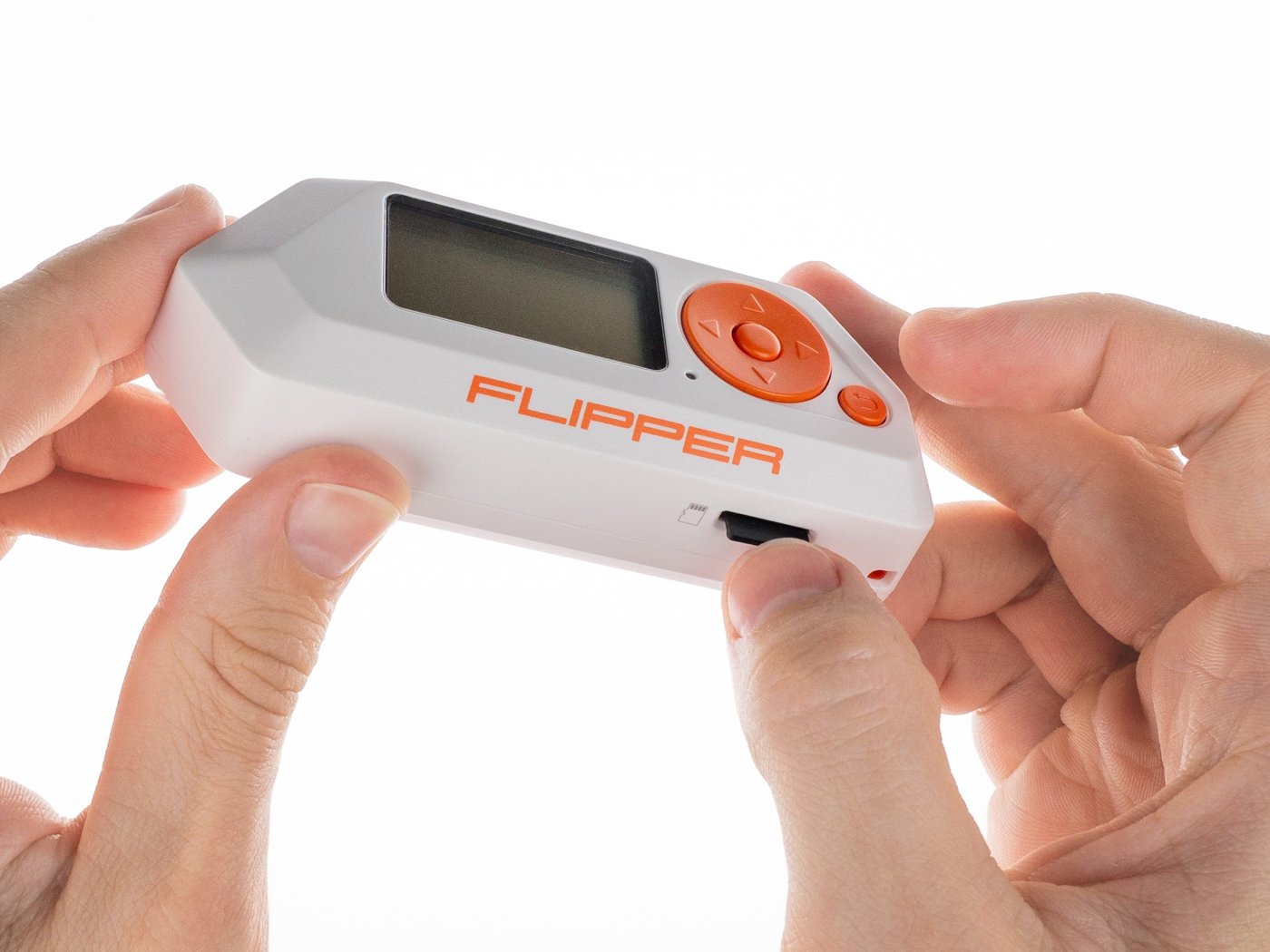
microSD card, FAT32, exposed via SPI from the MCU. Apps, payloads, captured signals, NFC dumps, asset packs, all assets live on the SD. Internal flash holds only the firmware itself. Performance limit is the SPI clock; large NFC dumps and IR file transfers are noticeably faster when you pull the card out and use a real reader.
2.8.3 USB
USB 2.0 full-speed (12 Mb/s) via the STM32WB55’s built-in PHY. Default descriptor presents three interfaces: a CDC ACM (serial console / RPC), a VCP-like for the firmware update protocol, and on FW 1.0 the USB HID for BadUSB. The HID interface comes up only when a BadUSB or HID app is foregrounded — the device doesn’t enumerate as a keyboard at all times.
2.8.4 Audio
Speaker driven via PWM from a TIM channel. A simple piezo, ~2 kHz fundamental — usable for boot sounds, simulated Morse playback, and the notorious “Music Player” feature. There is no audio DAC and no microphone. External I²S DAC modules (Vol 9 §audio) plug into the GPIO header for better audio.
2.9 The 18-pin GPIO Header
The full pinout is in Vol 7 §pinout — the canonical table. Summary here for context:
- Pins 1, 9 — 5 V (switched), 3.3 V (always-on) rails
- Pins 8, 11, 18 — GND
- Pins 10, 12 — SWCLK, SWDIO (PA14, PA13) — full SWD debug; this is what an ST-Link or Black Magic Probe attaches to
- Pins 2–7 + 15, 16 — general GPIO with alternate functions for SPI, I²C, ADC, DAC, and timer outputs
- Pin 13, 14 — USART1 TX/RX (PB6, PB7) — used by most ESP32-based Wi-Fi modules
- Pin 17 — 1-Wire (shared with iButton pad)
All I/Os are 3.3 V tolerant only — feeding a 5 V signal into them will damage the MCU. Each pin has an internal 51 Ω series resistor for ESD, sources up to 20 mA per pin, total budget ≤ 5 W or the PMIC trips.
2.10 The Wi-Fi Devboard Sub-PCB (separate schematic sheet)
The official WiFi Devboard is a separate PCB that mates with a USB-C-to- USB-C cable to the Flipper or via a 6-pin debug header on the bottom of the Flipper. It has its own schematic sheet in the F7B9C6 documents.
Key facts:
- MCU: ESP32-S2 WROVER (single-core 240 MHz Tensilica, 320 KB SRAM, 4 MB external flash, 8 MB external PSRAM).
- Stock firmware: Black Magic Probe — turns the board into a GDB-server-over-USB SWD probe. This is genuinely useful and underutilized — see Vol 7 §debugging.
- Reflashable to: Marauder (Wi-Fi attacks), FlipperHTTP (JSON/HTTP bridge for FAPs), or any custom ESP32-S2 Arduino/IDF binary.
- The two firmwares — Marauder and Black Magic — can’t coexist. Pick one per session.
Full module chapter in Vol 8 §wifi-devboard.
2.11 Production-Rev Notes (F7B9C6)
The F7B9C6 silkscreen on the back of the board is the production hardware revision. Earlier revs (E1B0E0, E2A0A0) exist in beta-tester / internal hands but the production retail device is F7B9C6. The schematic PDFs on docs.flipper.net are for F7B9C6.
Component substitutions across batches are minor — the BQ25896 has been seen as both BQ25896 and BQ25896RGER (same die, different package marking); the SPI flash for the Wi-Fi Devboard has shipped from both Winbond and GigaDevice. None of these affect software compatibility.
2.12 What’s next
Vol 3 — Firmware ecosystem. How to install Official, Momentum, Xtreme, Unleashed, RogueMaster; the recovery workflow when you brick a device; the BLE re-pair 3-step; the module firmware pairing matrix that says which Flipper firmware pairs with which module firmware version of VGM, Game Over, AWOK V3, etc.
Footnotes
-
Flipper Devices, “Schematics of Flipper Zero”, https://docs.flipper.net/zero/development/hardware/schematic. Mirror PDF on the ST community forum at https://community.st.com/ysqtg83639. ↩
-
STMicroelectronics, STM32WB55RG datasheet, https://www.st.com/resource/en/datasheet/stm32wb55rg.pdf. ↩
-
STMicroelectronics, RM0434 — STM32WB-series Advanced Arm-based 32-bit MCUs reference manual, Rev 16 (Mar 2026), https://www.st.com/resource/en/reference_manual/rm0434-stm32wb-series-advanced-armbased-32bit-mcus-stmicroelectronics.pdf. ↩
-
STMicroelectronics, ES0394 — STM32WB55xx/STM32WB35Cx device errata, Rev 17 (Oct 2025). ↩
-
Texas Instruments, CC1101 Low-Power Sub-1 GHz RF Transceiver datasheet, literature ID SWRS061I, https://www.ti.com/lit/ds/symlink/cc1101.pdf. ↩
-
STMicroelectronics, ST25R3916 datasheet, https://www.st.com/resource/en/datasheet/st25r3916.pdf. ↩
-
Vishay Semiconductors, TSOP753.. miniature receiver for infrared remote control systems, doc 82494, https://www.vishay.com/doc?82494. ↩
Comments (0)